Possible wait state insertion – Altera IP Compiler for PCI Express User Manual
Page 337
Chapter :
B–19
Descriptor/Data Interface
August 2014
Altera Corporation
IP Compiler for PCI Express User Guide
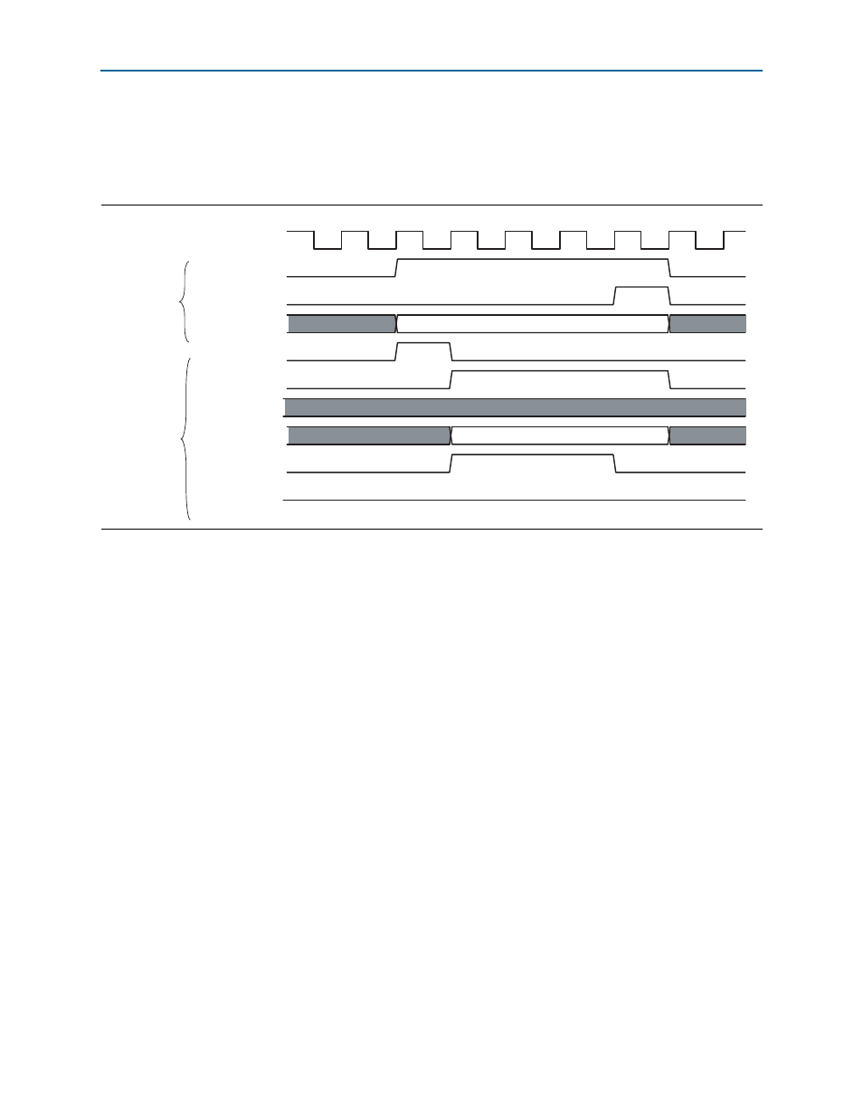
shows that the application layer must wait to receive an acknowledge
before write data can be transferred. Prior to the start of a transaction (for example,
tx_req
being asserted), note that the tx_ws signal is set low for the ×1 and ×4
configurations and is set high for the ×8 configuration.
Possible Wait State Insertion
If the IP core is not initialized with the maximum potential lanes, data transfer is
necessarily hindered. Refer to
. The application transmits a 32-bit memory
write transaction of 8 dwords. Address bit 2 is set to 0.
In clock cycle three, data transfer can begin immediately as long as the transfer buffer
is not full.
In clock cycle five, once the buffer is full and the IP core implements wait states to
throttle transmission; four clock cycles are required per transfer instead of one
because the IP core is not configured with the maximum possible number of lanes
implemented.
Figure B–15. TX Transaction Layer Not Ready to Accept Packet
clk
tx_req
tx_ack
tx_desc[127:0]
tx_dfr
tx_dv
tx_data[63:32]
tx_data[31:0]
tx_ws
tx_err
MEMWR32
DW0
Descriptor
Signals
Data
Signals
1
2
3
4
5
6
7
8
9