Variant>.v or .vhd, Figure 7–2, For more – Altera IP Compiler for PCI Express User Manual
Page 167
Chapter 7: Reset and Clocks
7–3
Reset Hard IP Implementation
August 2014
Altera Corporation
IP Compiler for PCI Express User Guide
qmegawiz -silent -wiz_override=”offset_cancellation_reset” <altgx_reconfig_filename.v>
After this signal is visible in your IP Compiler for PCI Express hard IP variation, you
can configure the general purpose PLL to generate the fixedclk, reconfig_clk, and
pll_locked
signals to meet the requirements described here. Altera recommends that
you use the _plus file and configure the PLL that supports the use of the internal reset
logic.
f
Refer to “PCI Express (PIPE) Reset Sequence” in th
chapter in volume 2 of the Stratix IV Device Handbook for a timing diagram illustrating
the reset sequence in Stratix IV devices.
1
To understand the reset sequence in detail, you can also review the
altpcie_rs_serdes.v
file.
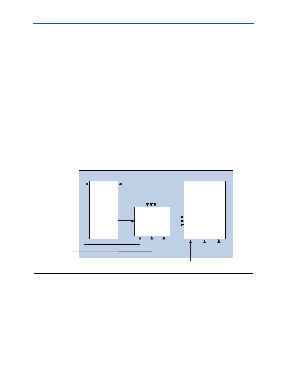
If you choose to implement your own reset circuitry, you must design logic to replace
the Transceiver Reset module shown in
.
provides a somewhat more detailed view of the reset signals in the
Figure 7–2. Reset Signals Provided for External Reset and Calibration Logic of the Hard IP Implementation
busy_altgxb_reconfig
Transceiver PHY IP Core
Hip_txclk 125 or 250 MHz
Transceiver Reset
Refclk
100 MHz
cal_blk_clk
50 MHz
fixedclk
125 MHz
PCI Express
Hard IP
dl_ltssm[4:0]
npor
pld_clk
125 or 250 MHz
tx_digitalreset
rx_analogreset
rx_digitalreset
rx_freqlocked
pll_locked
rx_pll_locked
or .vhd
or .vhd
altpcie_rs_serdes.v
or .vhd