Bit ddr mode, N in, Figure 14–2 – Altera IP Compiler for PCI Express User Manual
Page 223
Chapter 14: External PHYs
14–3
External PHY Support
August 2014
Altera Corporation
IP Compiler for PCI Express User Guide
■
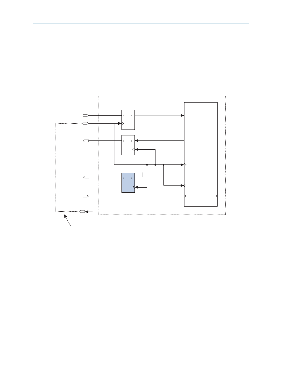
refclk
clocks a single data rate register for the incoming receive data
■
refclk
clocks the transmit data register (txdata) directly
■
refclk
also clocks a DDR register that is used to create a center aligned TXClk
This is the only external PHY mode that does not require a PLL. However, if the slow
tlp_clk
feature is used with this PIPE interface mode, then a PLL is required to create
the slow tlp_clk. In the case of the slow tlp_clk, the circuit is similar to the one
shown previously in
, the 16-bit SDR, but with TXClk output added.
8-bit DDR Mode
The implementation of the 8-bit DDR mode shown in
is included in the
file <variation name>.v or <variation name>.vhd and includes a PLL. The PLL inclock is
driven by refclk (pclk from the external PHY) and has the following outputs:
■
A zero delay copy of the 125 MHz refclk. The zero delay PLL output is used as
the clk125_in for the core and clocks a double data rate register for the incoming
receive data.
■
A 250 MHz early output. This is multiplied from the 125 MHz refclk is early in
relation to the refclk. Use the 250 MHz early clock PLL output to clock an 8-bit
SDR transmit data output register. A 250 MHz single data rate register is used for
the 125 MHz DDR output because this allows the use of the SDR output registers
in the Cyclone II I/O block. The early clock is required to meet the required clock
to out times for the common refclk for the PHY. You may need to adjust the phase
shift for your specific PHY and board delays. To alter the phase shift, copy the PLL
Figure 14–2. 16-bit SDR Mode with a 125 MHz Source Synchronous Transmit Clock
IP Compiler
for PCI Express
clk125_in
tlp_clk
refclk
clk125_out
ENB
A
D
Q
1
Q
4
refclk (pclk)
rxdata
txdata
clk125_out
External connection in user logic
clk125_in
ENB
Q
Q
A
1
D
4
ENB
Q
Q
A
1
D
4
txclk (~refclk)
DDIO