Altera IP Compiler for PCI Express User Manual
Page 220
13–10
Chapter 13: Reconfiguration and Offset Cancellation
Transceiver Offset Cancellation
IP Compiler for PCI Express User Guide
August 2014
Altera Corporation
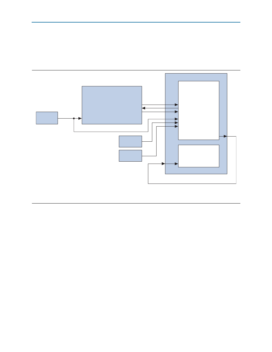
The chaining DMA design example instantiates the offset cancellation circuitry in the
file
shows the
connections between the ALTGX_RECONFIG instance and the ALTGX instance. The
names of the Verilog HDL files in this figure match the names in the chaining DMA
design example described in
Chapter 15, Testbench and Design Example
.
f
For more information about the ALTGX_RECONFIG megafunction refer to
. For more information
about the ALTGX megafunction refer to volume 2 of the
or
Figure 13–1. ALTGX_RECONFIG Connectivity
Note to
(1) The size of reconfig_togxb and reconfig_fromgxb buses varies with the number of lanes. Refer to
“Transceiver Control Signals” on
for details.
pld_clk
tx_clk_out
(ALTGX or ALT2GX
Megafunction )
(IP Compiler for
PCI Express)
reconfig_clk
cal_blk_clk
fixedclk
ALTGX_RECONFIG Megafunction
busy
reconfig_fromgxb[16:0]
reconfig_togxb[3:0]
busy
reconfig_fromgxb[16:0]
reconfig_togxb[3:0]
reconfig_clk
reconfig_clk
Reconfig
Clock Source
altpcie_reconfig_4sgx.v or .vhd
Reconfig
Clock Source
Fixed
Clock Source