Preparing the design for compilation, Design example wrapper file – Altera IP Compiler for PCI Express User Manual
Page 305
Chapter 16: Qsys Design Example
16–17
Preparing the Design for Compilation
August 2014
Altera Corporation
IP Compiler for PCI Express User Guide
Preparing the Design for Compilation
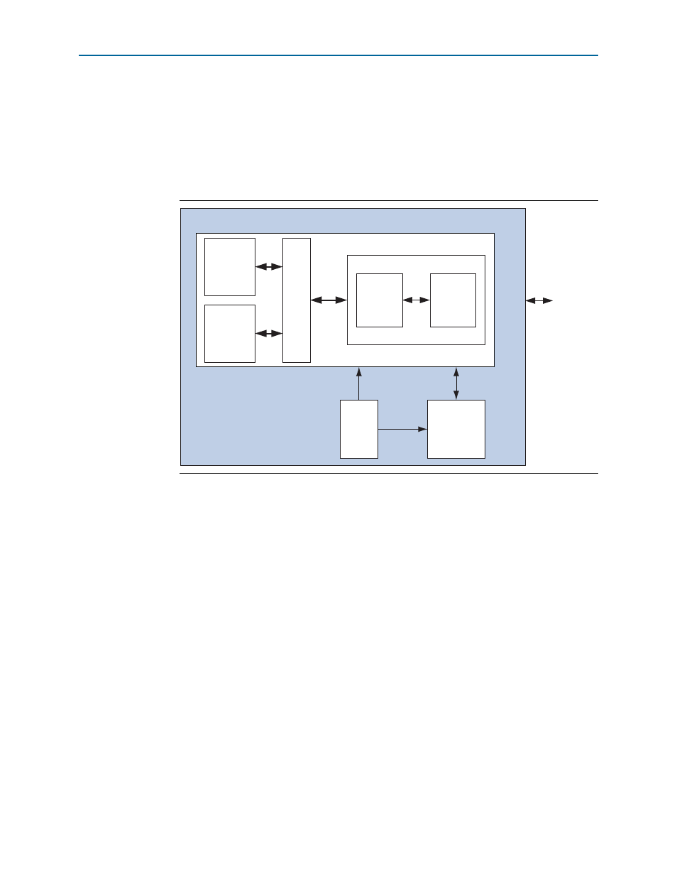
The Qsys design you generate and simulate in the preceding sections is a subsystem
of your Quartus II project. To configure and run in hardware, the Quartus II project
requires additional modules to support the IP Compiler for PCI Express.
shows a block diagram of the complete Quartus II project that you can compile,
configure, and run on a device.
Design Example Wrapper File
Altera provides a wrapper file s4gx_gen1x8_qsys_top.v that includes the required
connections and functionality for this design example. The file is located in your
Quartus II installation directory, in
/ip/altera/altera_pcie/altera_pcie_avmm/example_designs/s4gx_gen1x8
. You can
add it to the project with the design example Qsys system to create a Quartus II
project that configures and runs in hardware.
For more information about how the PLL and the altgxb_reconfig block connect to
and behave with the IP Compiler for PCI Express, refer to
. These modules are required to generate the 125 MHz
fixedclk
and 50 MHz reconfig_clk input clocks to the IP Compiler for PCI Express.
The Qsys design flow requires that you instantiate the altgxb_reconfig block outside
the Qsys system. When you create your own design, you can use the design example
wrapper file as a reference to help you write your own wrapper file.
Figure 16–6. Quartus II Project Block Diagram
Transaction,
Data Link,
and PHY
Layers
On-Chip
Memory
DMA
PLL
altgxb_reconfig
Qsys Generated Endpoint
Wrapper File
PCI Express
Link
fixedclk
pll_locked
reconfig_clk
reconfig_fromgxb
reconfig_togxb
reconfig_busy
PCI
Express
Avalon-MM
Bridge
Interconnect
IP Compiler for PCI Express