Bit ddr with a source synchronous txclk – Altera IP Compiler for PCI Express User Manual
Page 224
14–4
Chapter 14: External PHYs
External PHY Support
IP Compiler for PCI Express User Guide
August 2014
Altera Corporation
source file referenced in your variation file from the
<path>/ip/ip_compiler_for_pci_express/lib directory, where
directory in which you installed the IP Compiler for PCI Express, to your project
directory. Then use the parameter editor to edit the PLL source file to set the
required phase shift. Then add the modified PLL source file to your Quartus II
project.
■
An optional 62.5 MHz TLP Slow clock is provided for ×1 implementations.
An edge detect circuit detects the relationships between the 125 MHz clock and the
250 MHz rising edge to properly sequence the 16-bit data into the 8-bit output
register.
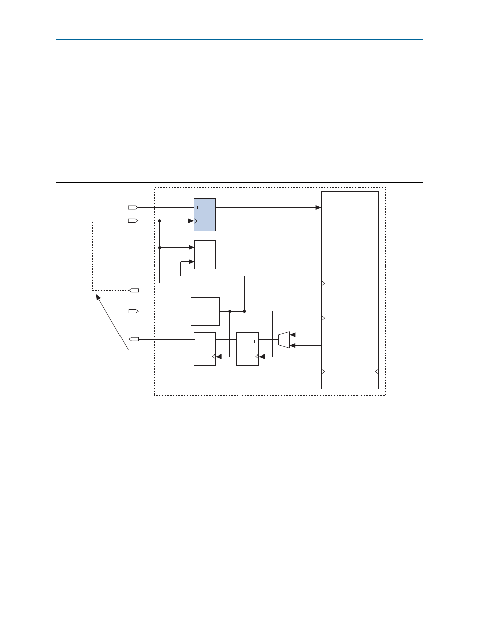
8-bit DDR with a Source Synchronous TXClk
shows the implementation of the 8-bit DDR mode with a source
synchronous transmit clock (TXClk). It is included in the file
<variation name>.vhd and includes a PLL. refclk (pclk from the external PHY) drives
the PLL inclock. The PLL inclock has the following outputs:
■
A zero delay copy of the 125 MHz refclk used as the clk125_in for the IP core
and also to clock DDR input registers for the RX data and status signals.
■
A 250 MHz early clock. This PLL output clocks an 8-bit SDR transmit data output
register. It is multiplied from the 125 MHz refclk and is early in relation to the
refclk
. A 250 MHz single data rate register for the 125 MHz DDR output allows
you to use the SDR output registers in the Cyclone II I/O block.
■
An optional 62.5 MHz TLP Slow clock is provided for ×1 implementations.
Figure 14–3. 8-Bit DDR Mode without Transmit Clock
IP Compiler
for PCI Express
clk125_in
tlp_clk
refclk
clk125_out
ENB
A
D
Q
1
Q
4
refclk (pclk)
rxdata
clk125_out
clk125_in
ENB
Q
Q
A
1
D
4
txdata
DDIO
out txclk
Mode 3
PLL
ENB
Q
Q
A
1
D
4
txdata_h
txdata_l
Edge
Detect
& Sync
clk250_early
tlp_clk
External connection
in user logic