Dependencies between receive signals – Altera IP Compiler for PCI Express User Manual
Page 329
Chapter :
B–11
Descriptor/Data Interface
August 2014
Altera Corporation
IP Compiler for PCI Express User Guide
■
The application layer deasserts rx_ws at clock cycle 11, thereby ending an
application interface-induced wait state.
Dependencies Between Receive Signals
describes the minimum and maximum latency values in clock cycles
between various receive signals.
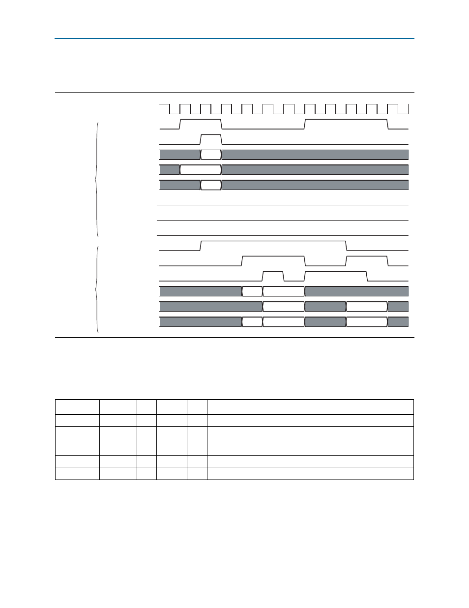
Figure B–9. RX Transaction with a Data Payload and Wait States Waveform
clk
rx_req
rx_ack
rx_desc[135:128]
rx_desc[127:64]
rx_desc[63:0]
rx_abort
rx_retry
rx_mask
rx_dfr
rx_dv
rx_ws
rx_data[63:32]
rx_data[31:0]
rx_be[7:0]
valid
CPLD 4 DW
valid
DW 0
DW 2
DW 1
DW 3
0xF0
0xFF
0x0F
1
2
3
4
5
6
7
8
9
10
11
12
Descriptor
Signals
Data
Signals
Table B–5. RX Minimum and Maximum Latency Values in Clock Cycles Between Receive Signals
Signal 1
Signal 2
Min
Typical
Max
Notes
rx_req
rx_ack
1
1
N
—
rx_req
rx_dfr
0
0
0
Always asserted on the same clock cycle if a data payload is present,
except when a previous data transfer is still in progress. Refer to
.
rx_req
rx_dv
1
1-2
N
Assuming data is sent.
rx_retry
rx_req
1
2
N
rx_req
refers to the next transaction request.