P_clk – Altera IP Compiler for PCI Express User Manual
Page 170
7–6
Chapter 7: Reset and Clocks
Clocks
IP Compiler for PCI Express User Guide
August 2014
Altera Corporation
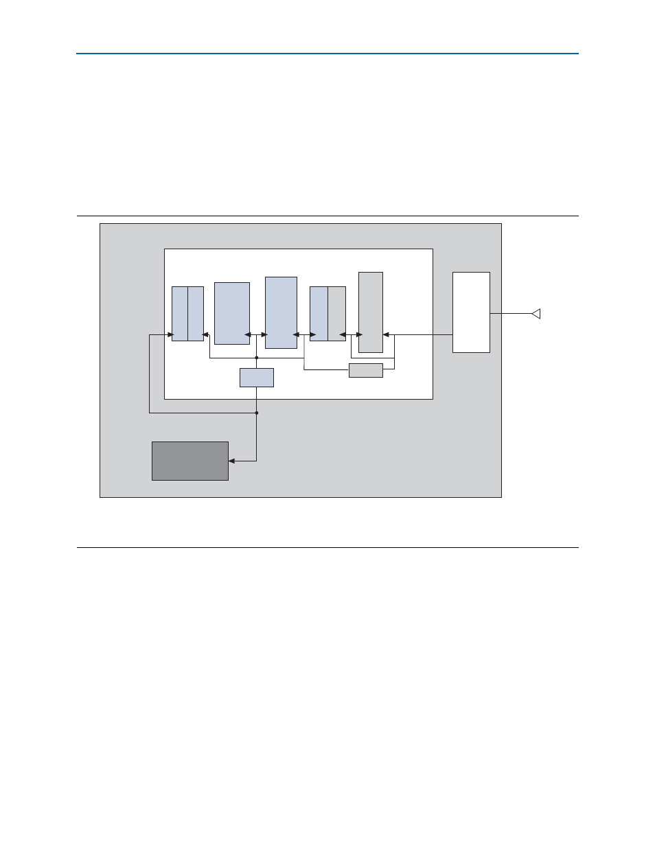
The IP core contains a clock domain crossing (CDC) synchronizer at the interface
between the PHY/MAC and the DLL layers which allows the data link and
transaction layers to run at frequencies independent of the PHY/MAC and provides
more flexibility for the user clock interface to the IP core. Depending on system
requirements, this additional flexibility can be used to enhance performance by
running at a higher frequency for latency optimization or at a lower frequency to save
power.
illustrates the clock domains.
indicates, there are three clock domains:
■
■
■
p_clk
The transceiver derives p_clk from the 100 MHz refclk signal that you must provide
to the device. The p_clk frequency is 250 MHz for Gen1 systems and 500 MHz for
Gen2. The PCI Express specification allows a +/- 300 ppm variation on the clock
frequency.
The CDC module implements the asynchronous clock domain crossing between the
PHY/MAC p_clk domain and the data link layer core_clk domain.
Figure 7–5. IP Compiler for PCI Express Clock Domains
Notes to
(1) The 100 MHz refclk can only drive the transceiver.
(2) If the core_clk_out frequency is 125 MHz, you can use this clock signal to drive the cal_blk_clk signal.
IP Compiler for PCI Express Hard IP Implementation - Clock Domains
Stratix IV GX Device
Data
Link
Layer
(DLL)
Trans-
action
Layer
(TL)
core_clk
pld_clk
core_clk_out
p_clk
100 MHz
refclk
PHY
MAC
User Application
Adapter
Trans-
ceiver
(1)
PLL
PLL
/2
Clock
Domain
Crossing
(CDC)
User Clock
Domain
(128-bit
mode only)