Datasheet, Features – Altera IP Compiler for PCI Express User Manual
Page 3
August 2014
Altera Corporation
1. Datasheet
This document describes the Altera
®
IP Compiler for PCI Express IP core. PCI Express
is a high-performance interconnect protocol for use in a variety of applications
including network adapters, storage area networks, embedded controllers, graphic
accelerator boards, and audio-video products. The PCI Express protocol is software
backwards-compatible with the earlier PCI and PCI-X protocols, but is significantly
different from its predecessors. It is a packet-based, serial, point-to-point interconnect
between two devices. The performance is scalable based on the number of lanes and
the generation that is implemented. Altera offers both endpoints and root ports that
are compliant with
and
for Gen1 or Gen2. Both endpoints and root ports can be
implemented as a configurable hard IP block rather than programmable logic, saving
significant FPGA resources. The IP Compiler for PCI Express is available in ×1, ×2, ×4,
and ×8 configurations.
shows the aggregate bandwidth of a PCI Express
link for Gen1 and Gen2 IP Compilers for PCI Express for 1, 2, 4, and 8 lanes. The
protocol specifies 2.5 giga-transfers per second for Gen1 and 5 giga-transfers per
second for Gen2. Because the PCI Express protocol uses 8B/10B encoding, there is a
20% overhead which is included in the figures in
provides
bandwidths for a single TX or RX channel, so that the numbers in
would be
doubled for duplex operation.
f
numbers
for the hard IP implementation in Stratix
®
IV GX and Arria
®
II GX devices.
Features
Altera’s IP Compiler for PCI Express offers extensive support across multiple device
families. It supports the following key features:
■
Hard IP implementation—
. The PCI Express
protocol stack including the transaction, data link, and physical layers is hardened
in the device.
■
■
■
Many device families supported. Refer to
.
■
The PCI Express protocol stack including transaction, data link, and physical
layer is implemented using FPGA fabric logic elements
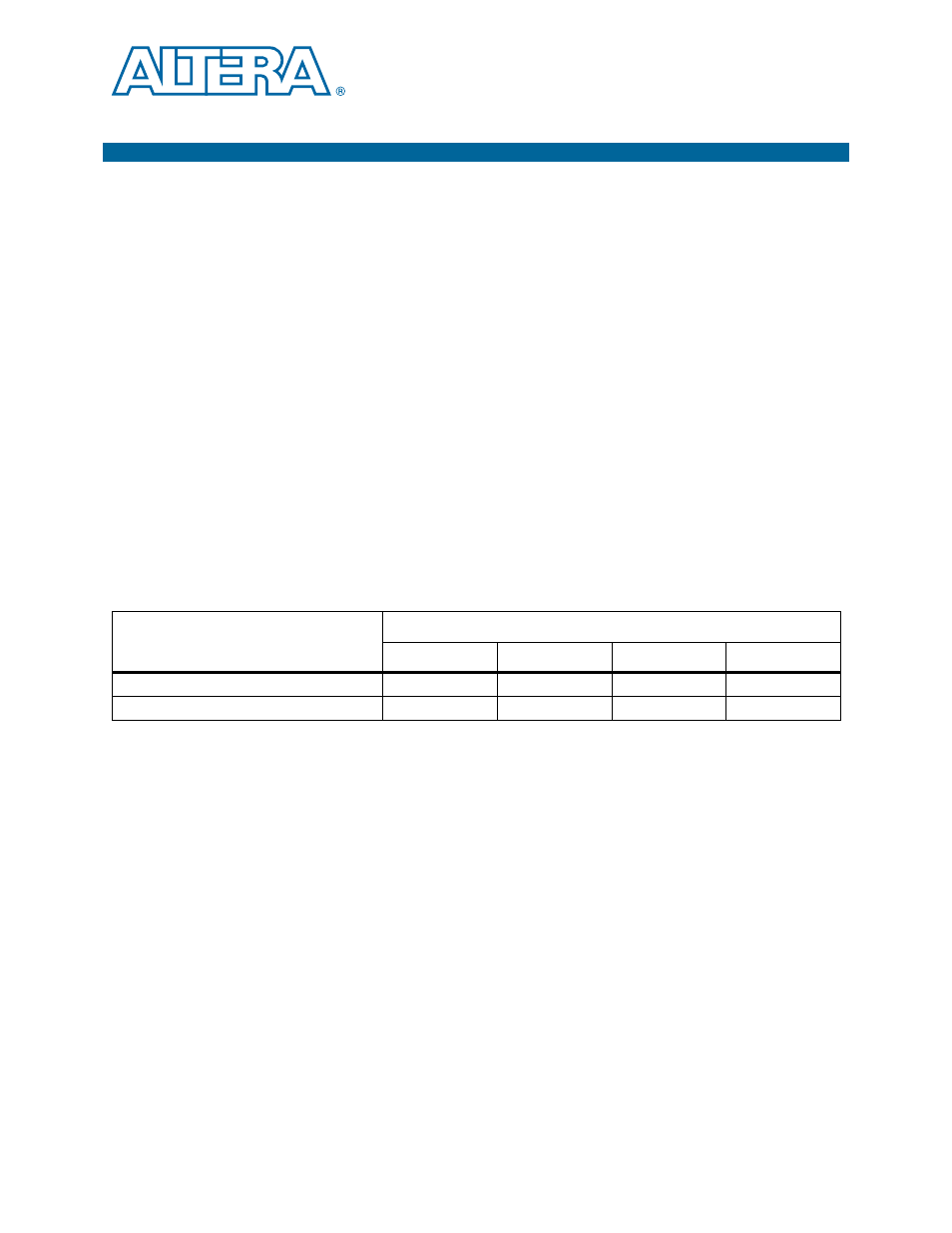
Table 1–1. IP Compiler for PCI Express Throughput
Link Width
×1
×2
×4
×8
PCI Express Gen1 Gbps (1.x compliant)
2
4
8
16
PCI Express Gen2 Gbps (2.0 compliant)
4
8
16
32
August 2014