Configuration space register access – Altera IP Compiler for PCI Express User Manual
Page 119
Chapter 5: IP Core Interfaces
5–33
Avalon-ST Interface
August 2014
Altera Corporation
IP Compiler for PCI Express User Guide
and global routing resources used for the pld_clk, the Quartus II software may have
difficulty avoiding hold time violations on the tl_cfg_ctl_wr and tl_cfg_sts_wr
signals. If hold time violations occur in your design, you can reduce the multicycle
setup time for these signals to 0. The exact time the signals are clocked is not critical to
the design, just that the signals are reliably sampled. There are instruction comments
in the
Configuration Space Register Access
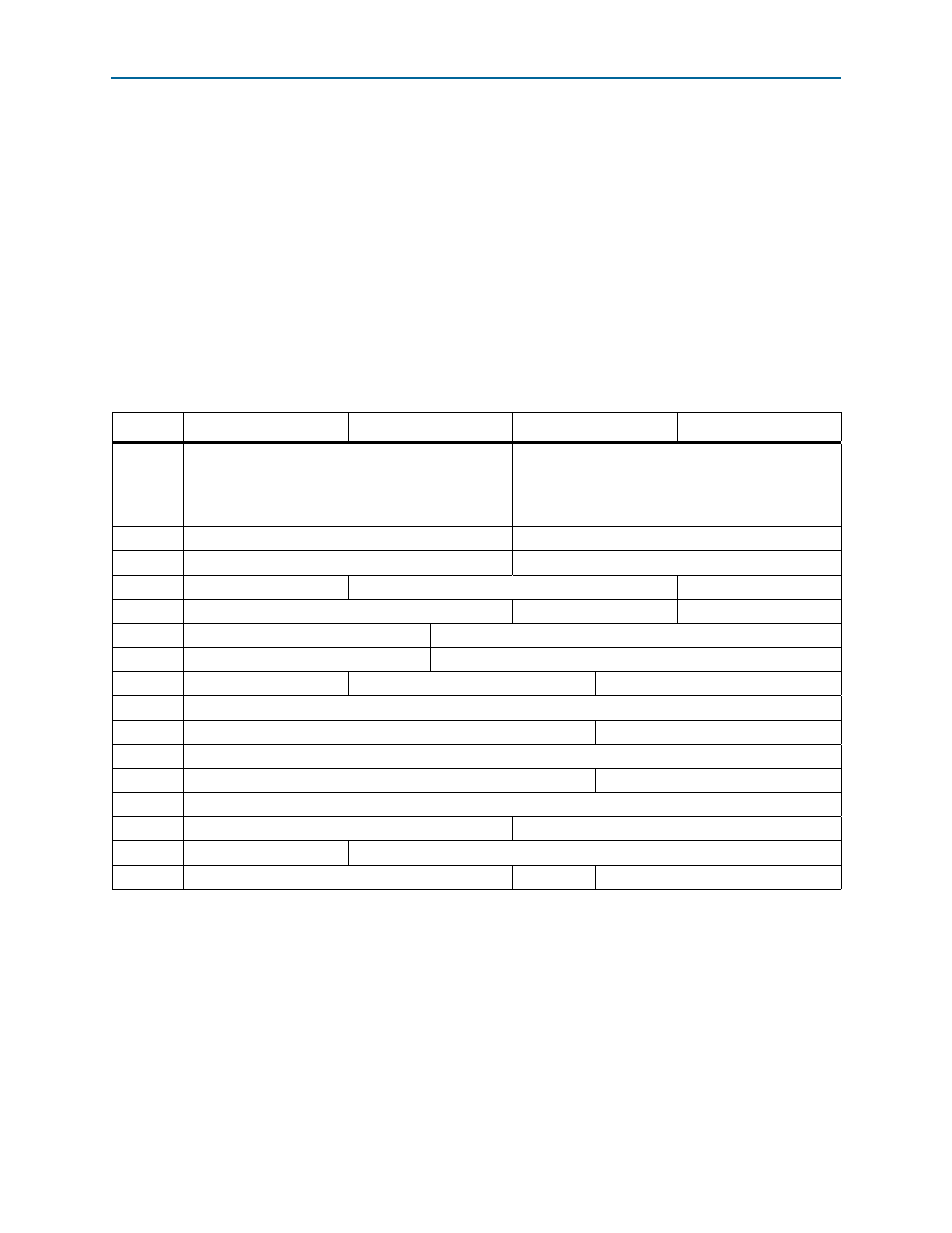
The tl_cfg_ctl signal is a multiplexed bus that contains the contents of configuration
space registers as shown in
. Information stored in the configuration space
is accessed in round robin order where tl_cfg_add indicates which register is being
accessed.
shows the layout of configuration information that is
multiplexed on tl_cfg_ctl.
Table 5–14. Multiplexed Configuration Register Information Available on tl_cfg_ctl
Address
31:24
23:16
15:8
7:0
0
cfg_devcsr[15:0]
cfg_dev2csr[15:0]
cfg_devcsr[14:12]=
Max Read Req Size
cfg_devcsr[7:5]=
Max Payload
1
cfg_slotcsr[31:16]
cfg_slotcsr[15:0]
2
cfg_linkscr[15:0]
cfg_link2csr[15:0]
3
8’h00
cfg_prmcsr[15:0]
cfg_rootcsr[7:0]
4
cfg_seccsr[15:0]
cfg_secbus[7:0]
cfg_subbus[7:0]
5
12’h000
cfg_io_bas[19:0]
6
12’h000
cfg_io_lim[19:0]
7
8h’00
cfg_np_bas[11:0] cfg_np_lim[11:0]
8
cfg_pr_bas[31:0]
9
20’h00000
cfg_pr_bas[43:32]
A
cfg_pr_lim[31:0]
B
20’h00000
cfg_pr_lim[43:32]
C
cfg_pmcsr[31:0]
D
cfg_msixcsr[15:0]
cfg_msicsr[15:0]
E
8’h00
cfg_tcvcmap[23:0]
F
16’h0000
3’b000
cfg_busdev[12:0]
Note to
:
(1) Items in blue are only available for root ports.
(2) This field is encoded as specified in Section 7.8.4 of th
.(3’b000–3b101 correspond to 128–4096 bytes).