Dma read cycles – Altera IP Compiler for PCI Express User Manual
Page 253
Chapter 15: Testbench and Design Example
15–21
Test Driver Module
August 2014
Altera Corporation
IP Compiler for PCI Express User Guide
3. Waits for the DMA write completion by polling the BFM share memory location
0x80c, where the DMA write engine is updating the value of the number of
completed descriptor. Calls the procedures rcmem_poll and msi_poll to determine
when the DMA write transfers have completed.
DMA Read Cycles
The procedure dma_rd_test used for DMA read uses the following three steps:
1. Configures the BFM shared memory with a call to the procedure
dma_set_rd_desc_data
which sets three descriptor tables (
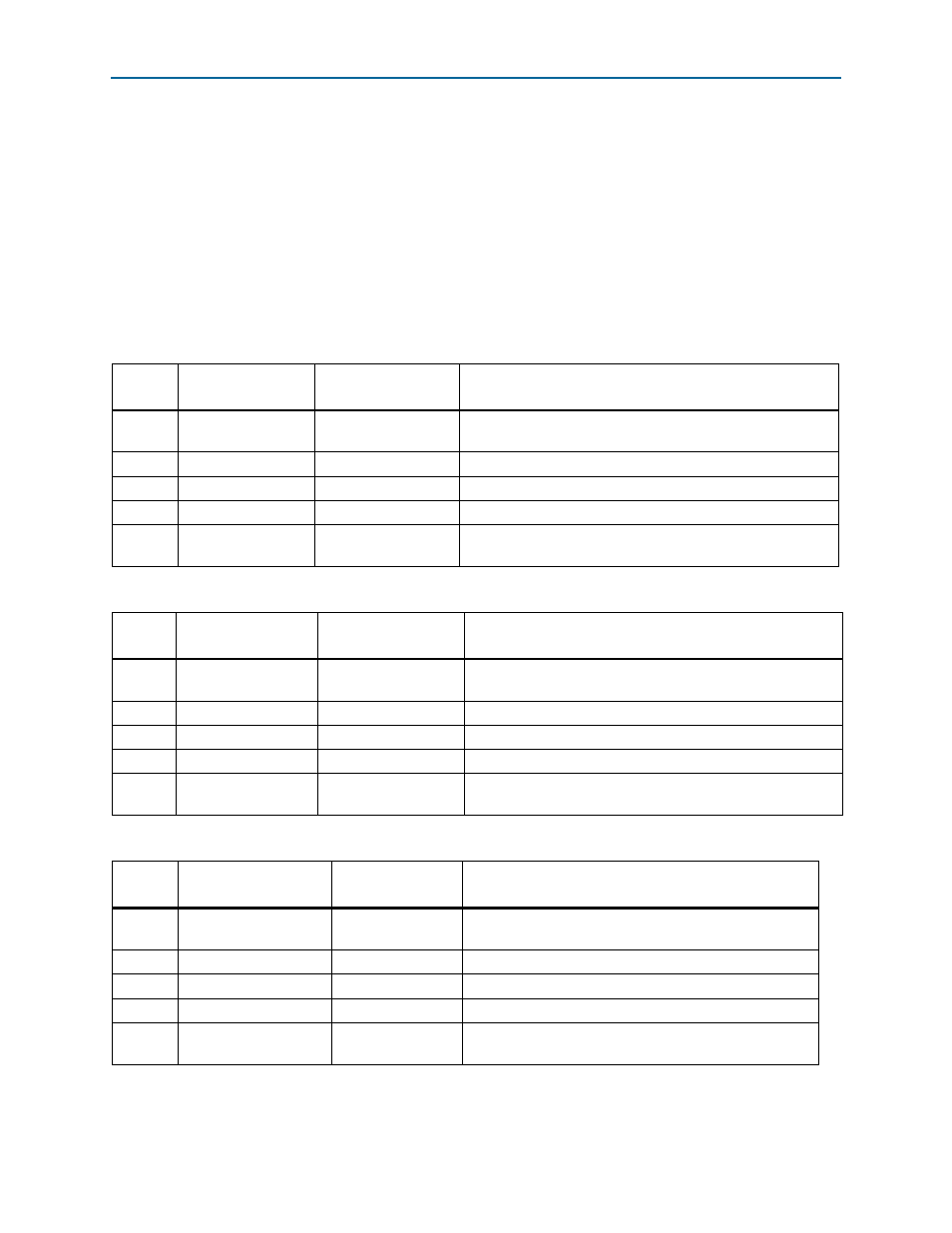
Table 15–18. Read Descriptor 0
Offset in BFM
Shared Memory
Value
Description
DW0
0x910 82
Transfer length in DWORDS and control bits as described in
DW1
0x914
3
Endpoint address value
DW2
0x918
0
BFM shared memory data buffer 0 upper address value
DW3
0x91c
0x8DF0
BFM shared memory data buffer 0 lower address value
Data
Buffer 0
0x8DF0
Increment by 1 from
0xAAA0_0001
Data content in the BFM shared memory from address: 0x89F0
Table 15–19. Read Descriptor 1
Offset in BFM
Shared Memory
Value
Description
DW0
0x920 1,024
Transfer length in DWORDS and control bits as described in
DW1
0x924
0
Endpoint address value
DW2
0x928
10
BFM shared memory data buffer 1 upper address value
DW3
0x92c
0x10900
BFM shared memory data buffer 1 lower address value
Data
Buffer 1
0x10900
Increment by 1 from
0xBBBB_0001
Data content in the BFM shared memory from address:
0x10900
Table 15–20. Read Descriptor 2
Offset in BFM Shared
Memory
Value
Description
DW0
0x930 644
Transfer length in DWORDS and control bits as described
in
DW1
0x934
0
Endpoint address value
DW2
0x938
0
BFM shared memory upper address value
DW3
0x93c
0x20EF0
BFM shared memory lower address value
Data
Buffer 2
0x20EF0
Increment by 1 from
0xCCCC_0001
Data content in the BFM shared memory from address:
0x20EF0