Pipe interface signals – Altera IP Compiler for PCI Express User Manual
Page 142
5–56
Chapter 5: IP Core Interfaces
Physical Layer Interface Signals
IP Compiler for PCI Express User Guide
August 2014
Altera Corporation
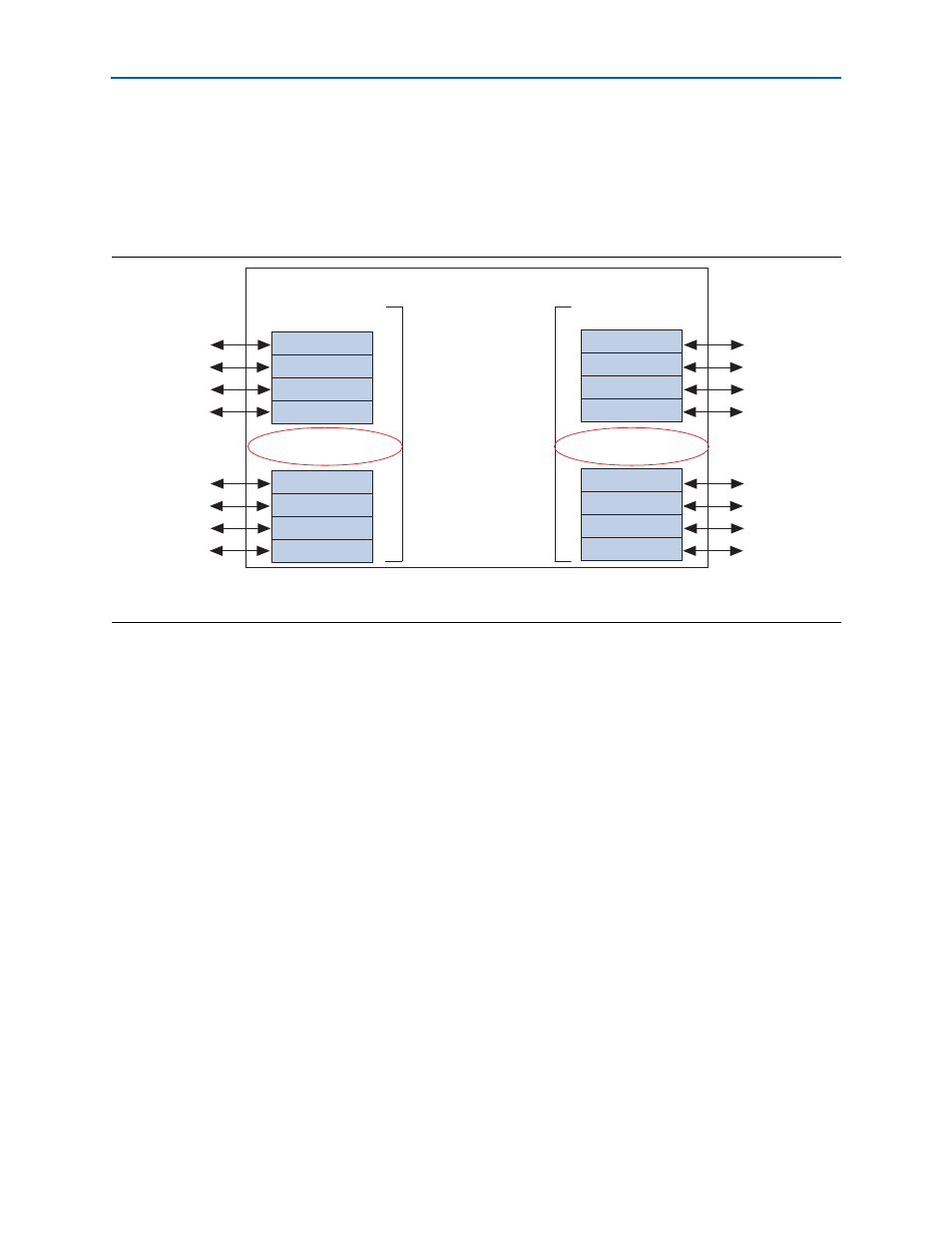
assigned in order to the pins associated with channels 0-3 of the slave transceiver
block. The signals rx_in[4]/tx_out[4] must be assigned to the pins associated with
channel 0 of the slave transceiver block, rx_in[5]/tx_out[5] must be assigned to the
pins associated with channel 1 of the slave transceiver block, and so on.
illustrates this connectivity.
1
You must verify the location of the master transceiver block before making pin
assignments for the hard IP implementation of the IP Compiler for PCI Express.
f
Refer to
for pin-out tables for all Altera devices in
, .txt, and .xls formats.
f
Refer to Vo
or Volume 2 of the
e information about the transceiver blocks.
PIPE Interface Signals
The ×1 and ×4 soft IP implementation of the IP core is compliant with the 16-bit
version of the PIPE interface, enabling use of an external PHY. The ×8 soft IP
implementation of the IP core is compliant with the 8-bit version of the PIPE interface.
These signals are available even when you select a device with an internal PHY so that
you can simulate using both the one-bit and the PIPE interface. Typically, simulation
is much faster using the PIPE interface. For hard IP implementations, the 8-bit PIPE
interface is also available for simulation purposes. However, it is not possible to use
the hard IP PIPE interface in an actual device.
signals used for a standard 16-bit SDR or 8-bit SDR interface. These interfaces are used
Figure 5–41. Two PCI Express ×8 Links in a Four-Transceiver Block Device
Note to
(1) This connectivity is specified in
PCI Express Lane 7
PCI Express Lane 6
PCI Express Lane 5
PCI Express Lane 4
PCI Express Lane 3
PCI Express Lane 2
PCI Express Lane 1
PCI Express Lane 0
Transceiver Block GXBL1
(Slave)
Channel3
Channel2
Channel1
Channel0
Transceiver Block GXBL0
(Master)
Second PCI
Express
(PIPE)
x8 Link
First PCI
Express
(PIPE)
x8 Link
Transceiver Block GXBR1
(Slave)
Transceiver Block GXBR0
(Master)
Channel3
Channel2
Channel1
Channel0
Channel3
Channel2
Channel1
Channel0
Channel3
Channel2
Channel1
Channel0
PCI Express Lane 7
PCI Express Lane 6
PCI Express Lane 5
PCI Express Lane 4
PCI Express Lane 3
PCI Express Lane 2
PCI Express Lane 1
PCI Express Lane 0
Stratix IV GX Device