Altera IP Compiler for PCI Express User Manual
Page 216
13–6
Chapter 13: Reconfiguration and Offset Cancellation
Dynamic Reconfiguration
IP Compiler for PCI Express User Guide
August 2014
Altera Corporation
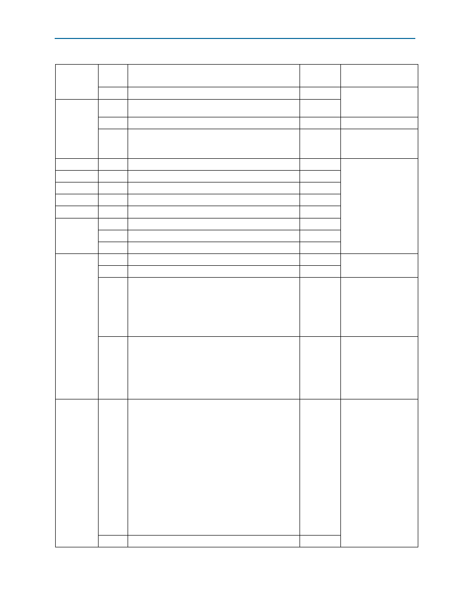
0x97
15:7 MSI-X table size
b’0
MSI-X Capability
Structure
0x98
1:0 Reserved.
—
4:2 MSI-X Table BIR.
b’0
15:5 MIS-X Table Offset.
b’0
MSI-X Capability
Structure
0x99
15:10 MSI-X PBA Offset.
b’0
—
0x9A
15:0 Reserved.
b’0
0x9B
15:0 Reserved.
b’0
0x9C
15:0 Reserved.
b’0
0x9D
15:0 Reserved.
b’0
0x9E
3:0 Reserved.
7:4 Number of EIE symbols before NFTS.
b’0100
15:8 Number of NFTS for separate clock in Gen2 rate.
b’11111111
0x9F
7:0 Number of NFTS for common clock in Gen2 rate.
b’11111111
Link Control register 2
8 Selectable de-emphasis.
b’0
12:9
PCIe Capability Version.
b’0010
PCI Express capability
register
b’0000: Core is compliant to PCIe Specification 1.0a or
1.1.
b’0001: Core is compliant to PCIe Specification 1.0a or
1.1.
b’0010: Core is compliant to PCIe Specification 2.0.
15:13
L0s exit latency for common clock.
Gen1: ( N_FTS (of separate clock) + 1 (for the SKIPOS)
) * 4 * 10 * UI (UI = 0.4 ns).
Gen2: [ ( N_FTS2 (of separate clock) + 1 (for the
SKIPOS) ) * 4 + 8 (max number of received EIE) ] * 10
* UI (UI = 0.2 ns).
b’110
Link Capability register
0xA0
2:0
L0s exit latency for separate clock.
Gen1: ( N_FTS (of separate clock) + 1 (for the SKIPOS)
) * 4 * 10 * UI (UI = 0.4 ns).
Gen2: [ ( N_FTS2 (of separate clock) + 1 (for the
SKIPOS) ) * 4 + 8 (max number of received EIE) ] * 10
* UI (UI = 0.2 ns).
b’000 – Less than 64 ns.
b’001 – 64 ns to less than 128 ns.
b’010 – 128 ns to less than 256 ns.
b’011 – 256 ns to less than 512 ns.
b’100 – 512 ns to less than 1 µs.
b’101 – 1 µs to less than 2 µs.
b’110 – 2 µs to 4 µs.
b’111 – More than 4 µs.
b’110
Link Capability register
15:3 Reserved.
0x0000
Table 13–1. Dynamically Reconfigurable Registers in the Hard IP Implementation (Part 5 of 7)
Address
Bits
Description
Default
Value
Additional Information