Icm block diagram, Rx datapath, Tx datapath – Altera IP Compiler for PCI Express User Manual
Page 347: Msi datapath
Chapter :
B–29
Incremental Compile Module for Descriptor/Data Examples
August 2014
Altera Corporation
IP Compiler for PCI Express User Guide
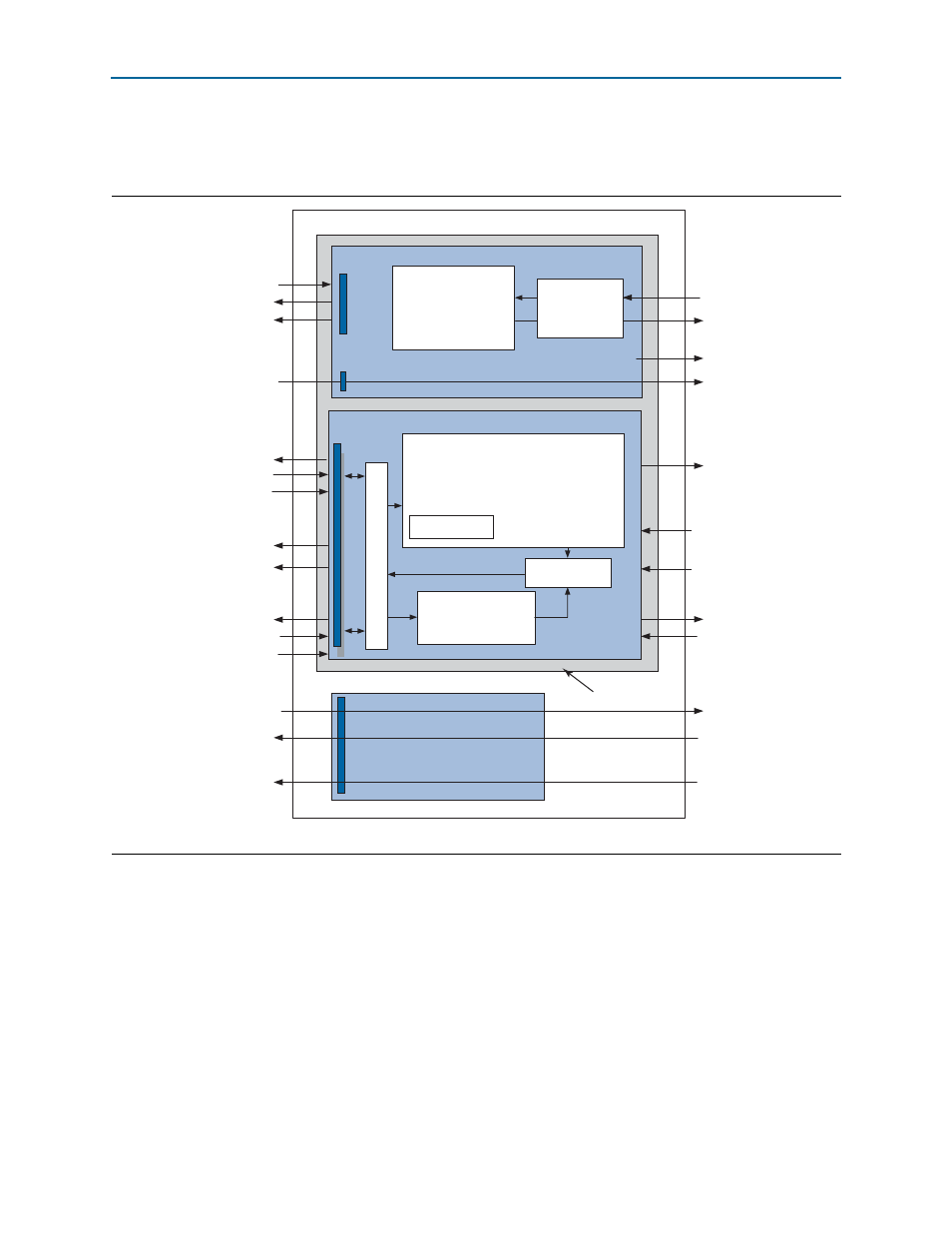
ICM Block Diagram
The ICM comprises four main sections:
■
■
■
■
All signals between the IP Compiler for PCI Express and the user application are
registered by the ICM. The design example implements the ICM interface with one
virtual channel. For multiple virtual channels, duplicate the RX and TX Avalon-ST
interfaces for each virtual channel.
Figure B–24. ICM Block Diagram
To PCI Express
Transaction Layer
1'b0
ICM Rx
To user application
(streaming interface )
rx_stream_ready0
rx_stream_valid0
rx_stream_data0
tx_stream_ready0
tx_stream_valid0
tx_stream_data0
msi_stream_ready0
msi_stream_valid0
msi_stream_data0
cpl_pending_icm
cpl_err_icm
pex_msi_num_icm
app_int_sts_icm
app_int_sts_ack_icm
cfg_busdev_icm
cfg_devcsr_icm
cfg_linkcsr_icm
cfg_tcvcmap_icm
cfg_msicsr_icm
test_out_icm
cpl_pending
cpl_err
pex_msi_num
app_int_sts
app_int_sts_ack
cfg_msicsr
cfg_busdev
cfg_devcsr
cfg_linkcsr
cfg_tcvcmap
test_out
app_msi_num
app_msi_req
app_msi_tc
app_msi_ack
tx_ack0
tx_ws0
tx_req0
tx_desc0
tx_dfr0
tx_dv0
tx_data0
tx_err0
cpl_err0
cpl_pending0
rx_retry0
rx_abort0
rx_mask0
rx_ack0
rx_ws0
rx_req0
rx_desc0
rx_dfr0
rx_dv0
rx_data0
tx_cred0
rx_stream_mask0
tx_stream_mask0
tx_stream_mask0
tx_stream_cred0
ICM Sideband
Msg Handler
(ack & drop
messages)
Incremental Compile Module (ICM)
Instantiate
one per
virtual
channel
ICM Tx
F
I
F
O
Read Control
Arbitration
Reg
Reg
Reg
Reg
Avalon-ST Rx
Conversion
Avalon-ST Tx Conversion
NP Bypass
Avalon-ST MSI
Conversion