4 general-purpose registers, Chapter 3 cpu function – NEC PD78214 User Manual
Page 76
47
Chapter 3 CPU Function
3
Fig. 3-9 Data Saved to the Stack Area
Fig. 3-10 Data Restored from the Stack Area
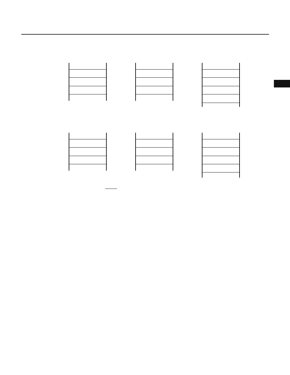
PUSH rp instruction
Stack
Register pair, low
Register pair, high
SP – 2
SP – 1
SP
⇒
SP
← SP – 2
↑
↑
CALL, CALLF, and CALLT instructions
Stack
PC7-PC0
PC15-PC8
SP – 2
SP – 1
SP
⇒
SP
← SP – 2
↑
↑
Interrupt
Stack
PC7-PC0
PC15-PC8
SP – 2
SP – 1
SP
⇒
SP
← SP – 3
↑
↑
PSW
SP – 3
↑
SP
⇒
POP rp instruction
Stack
Register pair, low
Register pair, high
SP + 1
SP + 2
↓
↓
RET instruction
Stack
PC7-PC0
PC15-PC8
RETI instruction
Stack
PC7-PC0
PC15-PC8
SP + 1
SP + 2
↓
↓
PSW
SP + 3
↓
SP
← SP + 2
SP
⇒
SP + 1
SP + 2
↓
↓
SP
← SP + 2
SP
⇒
SP
← SP + 3
Cautions 1. In stack addressing, the entire 64K bytes can be accessed. A stack area cannot be mapped in the SFR area or internal ROM area.
2. The SP becomes undefined when RESET is input. Meanwhile, nonmaskable interrupts can be acknowledged immediately after
a reset is released. If a nonmaskable interrupt request occurs, while the SP is undefined, immediately after a reset is released,
an unpredictable operation may be carried out. To minimize this danger, initialize the SP immediately after a reset is released.
For details, see Section 12.3.2.
3.2.4 General-Purpose Registers
(1) Configuration
General-purpose registers are mapped to special addresses (0FEE0H to 0FEFFH) in data memory. The
registers are grouped into four banks, each of which consists of eight 8-bit registers (X, A, C, B, E, D, L, H) (see
Fig. 3-11).