5 a/d conversion activated by hardware start, Chapter 8 a/d converter – NEC PD78214 User Manual
Page 264
235
Chapter 8 A/D Converter
8
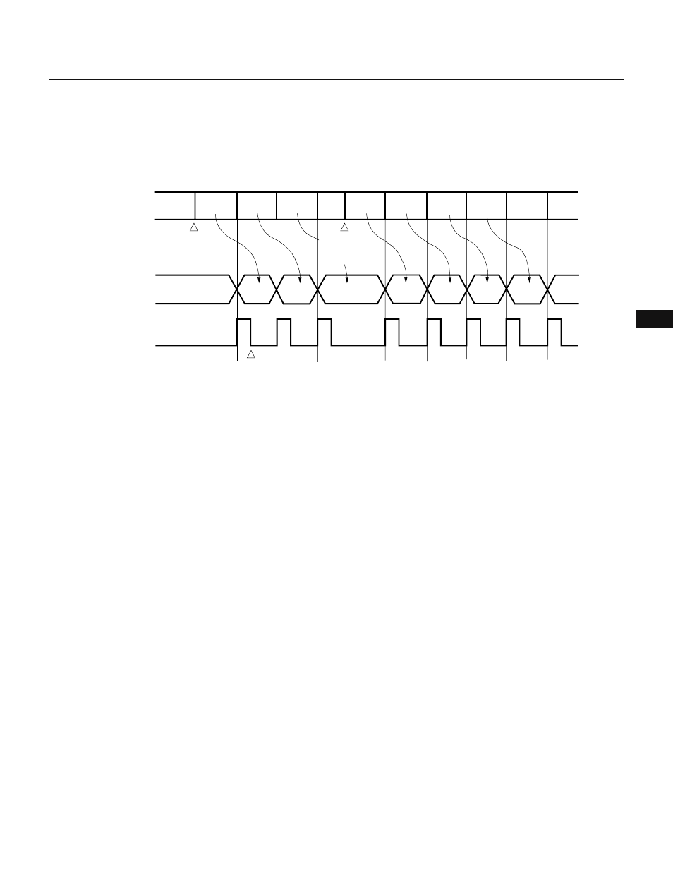
(2) Scan-mode A/D conversion
When triggered, conversion begins with the signal input to the AN0 pin. When the conversion sequence for
the AN0 pin is completed, the signal at the next analog input pin is converted. Each time a conversion
sequence is completed, an interrupt request (INTAD) is generated.
Fig. 8-9 Software-Started Scan-Mode A/D Conversion
8.3.5 A/D Conversion Activated by Hardware Start
Hardware can start A/D conversion by setting both the TRG and CS bits of the ADM register to 1. When they are
set to 1, the A/D converter is ready to receive an external signal. A/D conversion begins when a valid edge arrives
at the INT5 pin (pin P26).
After A/D conversion is started, if another valid edge arrives at the INT5 pin, the current sequence of A/D conversion
is stopped, and another sequence of conversion is started from the beginning, in accordance with the current ADM
register contents.
If such a value that both the TRG and CS bits are set to 1 is written to the ADM register again during A/D conversion
(the CS bit is 1), the current conversion sequence (including a wait period for an external signal) is stopped. The
converter stands by, until a valid edge arrives at the INTP5 pin in the mode of A/D conversion specified by the
written value. When a valid edge arrives, conversion starts.
By using this function, A/D conversion can be synchronized with an external signal.
When one A/D conversion sequence is completed, another conversion sequence is started immediately in an
operating mode set in the ADM register (the converter does not wait for the input from the INTP5 pin). Conversion
continues until an instruction that writes to the ADM register is executed or until a valid edge arrives at the INTP5
pin.
Cautions 1. Eight to twelve system clocks are required from when a valid edge appears at the INTP5 pin until A/D conversion is actually
started. Take this delay into consideration when designing your application. See Chapter 11 for details on the edge detection
function.
2. When A/D conversion is already activated by hardware start (by a valid edge at the INTP5 pin), if another valid edge arrives at
the INTP5 pin, the A/D converter may malfunction. To be specific, the malfunction occurs if the valid edge arrives at the INTP5
pin when the previous conversion result is being stored in the A/D conversion result register (ADCR). In this case, an A/D
conversion end interrupt (INTAD) is generated. However, the value stored in the ADCR register is not the conversion result.
Instead, it is always 7FH (see Fig. 8-10).
Conversion
starts
CS
←1, TRG←0
AN0
ADCR
AN1
AN2
AN0
AN1
AN2
AN0
AN0
AN1
AN2
AN0
AN0
AN1
AN2
AN0
AN1
INTAD
ADM rewriting
CS
←1,
TRG
←0
Interrupt request
accepted
A/D conversion
(scans AN0 to
AN2)