Chapter 8 a/d converter – NEC PD78214 User Manual
Page 256
227
Chapter 8 A/D Converter
8
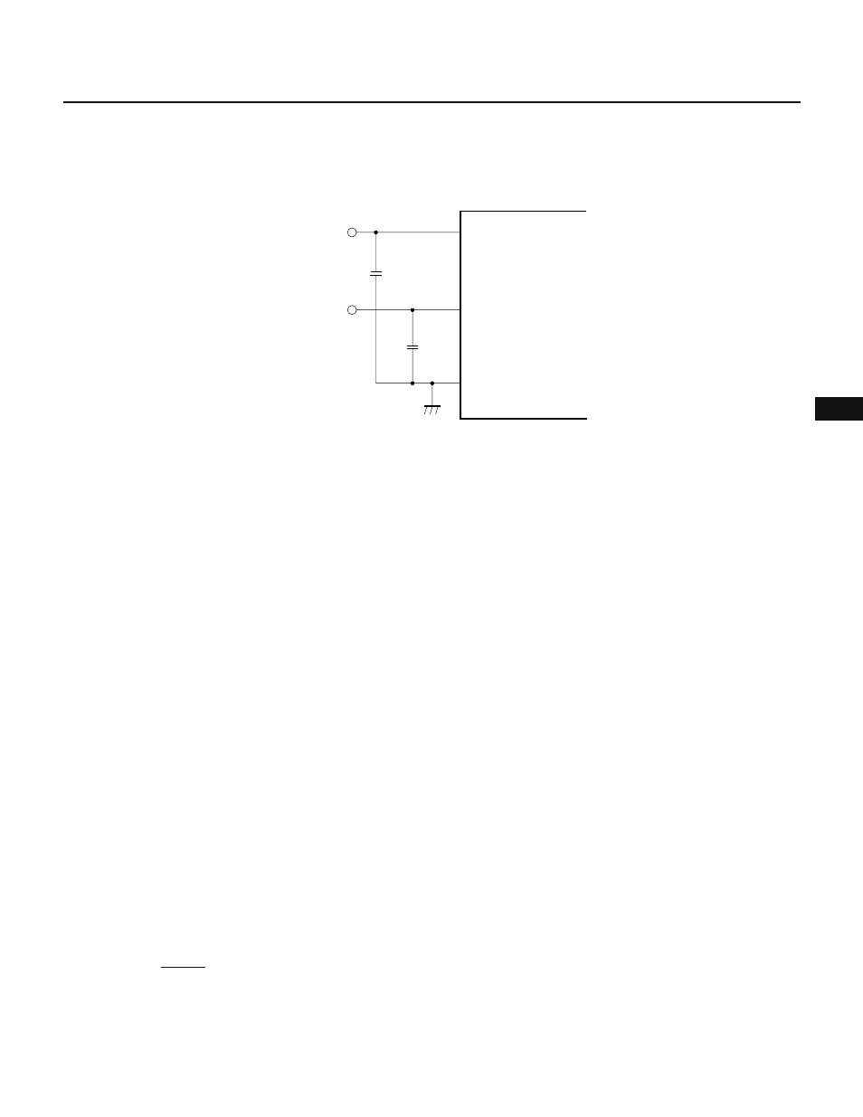
Cautions 1. To prevent malfunction due to noise, insert a capacitor between each analog input pins (AN0 through AN7) and the AV
SS
pin
and between the reference voltage input pin (AV
REF
) and the AV
SS
pin.
Fig. 8-2 Example of Capacitors Connected to the A/D Converter Pins
2. Do not apply a voltage out of the rated voltage range (AV
SS
through AV
REF
) to the A/D converter input pins. See Section 8.6
for details.
(1) Input circuit
The input circuit selects an input analog signal as specified by the A/D converter mode register (ADM) and
sends the signal to the sample and hold circuit in accordance with a specified operating mode.
(2) Sample and hold circuit
The sample and hold circuit samples each of the analog signals successively sent from the input circuit and
retains the analog signals during A/D conversion.
(3) Voltage comparator
The voltage comparator compares the potential differences between the analog inputs and the voltage taps
of the serial resistor string.
(4) Series resistor string
The series resistor string generates a voltage that matches the input analog signal voltage.
The series resistor string is connected between the reference voltage pin (AV
REF
) and the GND pin (AV
SS
) of
the A/D converter. It consists of 255 resistors, each having equal resistance, and two resistors, each having
half the resistance of the other 255 resistors. This configuration enables the voltage between the AV
REF
and
AV
SS
pins to be divided into 256 steps.
A voltage tap of the resistor string is selected by a tap selector, which is controlled by the SAR register.
(5) Successive approximation register (SAR)
When the voltage at one of the voltage taps of the serial resistor string matches the analog input voltage, this
8-bit register is set with the corresponding data on a bit-by-bit basis, starting at the most significant bit (MSB).
When the SAR is set up to the least significant bit (LSB), the SAR contents (conversion result) are sent to the
A/D conversion result register (ADCR) and held there.
(6) A/D conversion result register (ADCR)
This 8-bit register holds the A/D conversion result. Each time A/D conversion ends, this register is loaded with
the conversion result received from the SAR.
When the RESET signal is input, the contents of the register become undefined.
AV
REF
Analog input
Reference
voltage input
100-
500pF
AN0-AN7
AV
SS
PD78214
µ