NEC PD78214 User Manual
Page 59
30
µ
PD78214 Sub-Series
(6) P60 to P67 (port 6): Output (P60 to P63) and tristate inputs/outputs (P64 to P67)
Port 6 is an eight-bit I/O port with output latches. Pins P64 to P67 are provided with software-programmable
pull-up resistors.
The pins of port 6 also function as control signal input pins, as listed in Table 2-3. To use these pins as control
signal input pins, set up is required.
In the case of the
µPD78213, P64 and P65 act as an RD output and WR output, respectively.
When the RESET signal is applied, P60 to P63 go low and P64 to P67 function as an input port (the outputs
become high impedance). The contents of the output latches become undefined at the four high-order bits
and 0H at the four low-order bits.
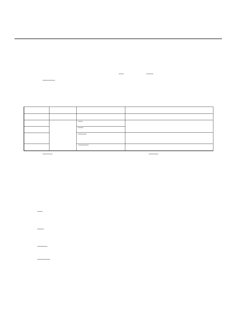
Table 2-3 Port 6 Operating Mode
P60-P63
P64
P65
P66
P67
A16-A19 output
RD output
WR output
WAIT input/AN6 input
REFRQ output/AN7 input
Pin
Port mode
Control signal I/O mode
Operation required to assign pins as control signal pins
For the
µPD78213, specify external memory expansion
mode using bits MM2 to MM0 of the MM register.
Set the MM6 bit of the MM register to 1.
Set the PW register, or bits PWn1 and PWn0 (n = 2
and 3) of the MM register and P66 to input mode.
Set the RFEN bit of the RFM register to 1.
Output port
Input/output
port
Caution While the RESET signal is being applied, P60 to P63 is high impedance. When the RESET signal is released, the output of these pins
is low level. Design the peripheral circuit so that it operates normally when pins P60 to P63 initially output low level.
Remark For details, see Chapter 13.
(a) Port mode
P60 to P63 are an output port. Each of pins P64 to P67 can be used for input or output by specifying the
port-6 mode register (PM6) accordingly.
(b) Control signal I/O mode
(i) A16 to A19 (address bus)
High-order address bus output when the external memory area is expanded (10000H to FFFFFH). The
memory expansion register (MM) controls these pins.
(ii) RD (read strobe)
Strobe signal output used for reading the external memory. In the case of the
µPD78213, the MM
register controls this pin.
(iii) WR (write strobe)
Strobe signal output used for writing to the external memory. In the case of the
µPD78213, the MM
register controls this pin.
(iv) WAIT (wait)
Wait signal input. The programmable wait control (PW) register or MM register controls this pin.
(v) REFRQ (refresh request)
Used for outputting refresh pulses to the external pseudo-static memory. The refresh mode register
(RFM) controls this pin.
(vi) AN6 and AN7 (analog input)
Analog inputs to the A/D converter.
(7) P70 to P75 (port 7): Input
Port 7 is a six-bit input port. Its pins also function as analog input pins (AN0 to AN5) for the A/D converter.
Signals applied to these pins can be read and these pins can be tested regardless of whether these pins are
acting as secondary function pins.