2 select mode – NEC PD78214 User Manual
Page 261
232
µ
PD78214 Sub-Series
(3) A/D conversion time
The time required for A/D conversion is determined by the system clock frequency (f
CLK
) and the FR bit of the
ADM register. To maintain A/D conversion accuracy above a certain level, it is necessary to set the FR bit as
listed in Table 8-2 according to the system clock frequency.
This A/D conversion time includes all the time required for one A/D conversion sequence and the sampling
time.
Table 8-2 shows the conversion time and sampling time.
Table 8-2 A/D Conversion Time
4 MHz < f
CLK
≤ 6 MHz
2 MHz
≤ f
CLK
≤ 4 MHz
0
1
180/f
CLK
(30
µs to 45 µs)
120/f
CLK
(30
µs to 60 µs)
36/f
CLK
(6
µs to 9 µs)
24/f
CLK
(6
µs to 12 µs)
System clock (f
CLK
)
range
FR bit
Conversion time
Sampling time
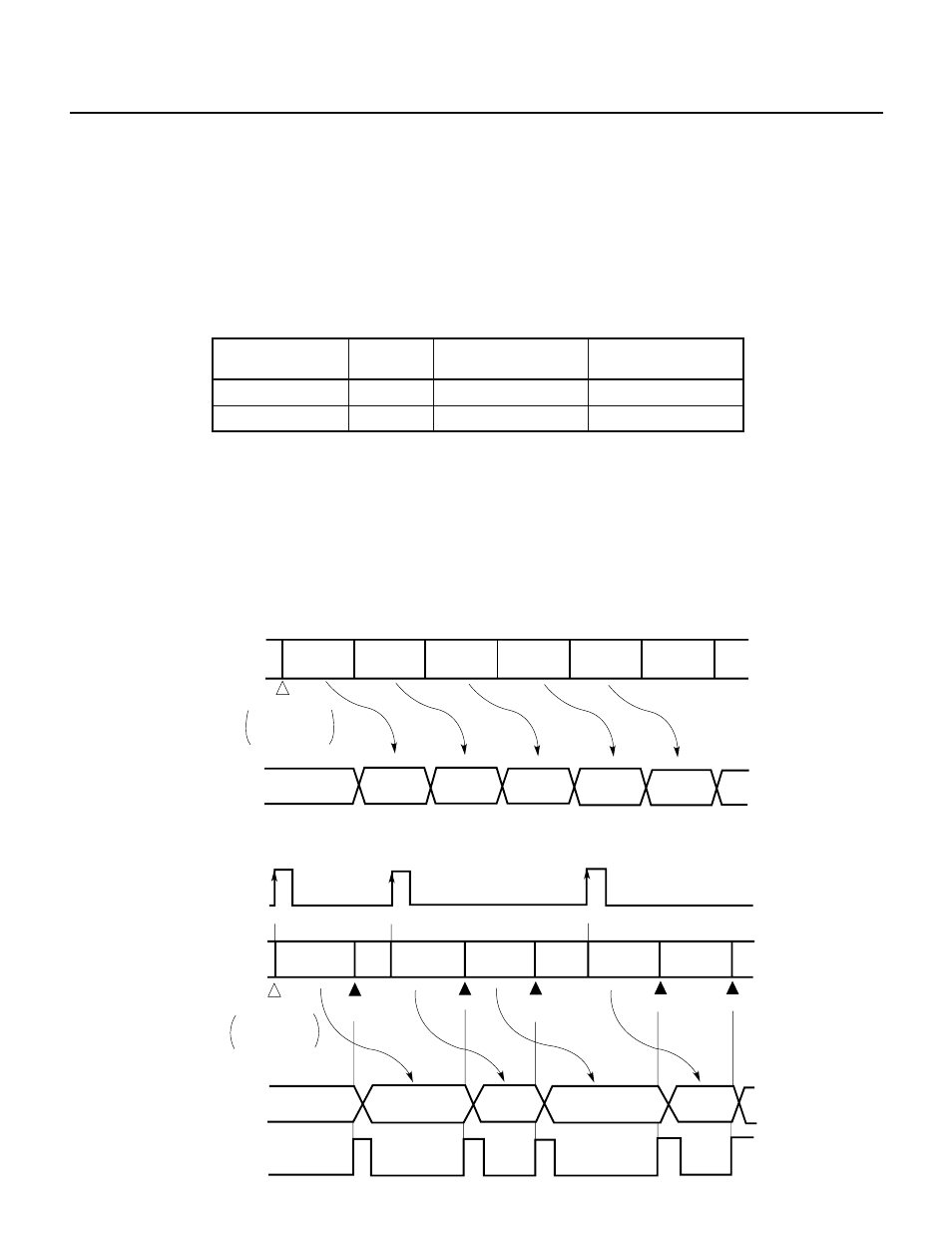
8.3.2 Select Mode
Bits 1 through 3 (ANI0 through ANI2) of the ADM register specify one analog input pin. A/D conversion is repeated
for the specified pin. The resultant digital data is stored in the A/D conversion result register (ADCR).
If bit 6 (TRG) of the ADM register is set to enable an external trigger, an A/D conversion end interrupt request
(INTAD) is generated.
Fig. 8-6 Select Mode Operation Timing
(a) TRG bit
← 0
A/D
conversion
Conversion starts
CS
←1
MS
←1
ANI2-0
←011
ADCR
AN3
AN3
AN3
AN3
AN3
AN3
AN3
AN3
AN3
AN3
AN3
(b) TRG bit
← 1
AN0
AN0
AN0
AN0
Conversion starts
AN0
AN0
AN0
AN0
AN0
AN0
CS
←1
MS
←1
ANI2-0
←000
AN0
Initialization
Initialization
Initialization
INTP5
A/D
conversion
ADCR
INTAD
Conversion
end
Conversion
end
Conversion
end
Conversion
end
Conversion
end