5 block diagram, Chapter 1 general – NEC PD78214 User Manual
Page 46
17
Chapter 1 General
1
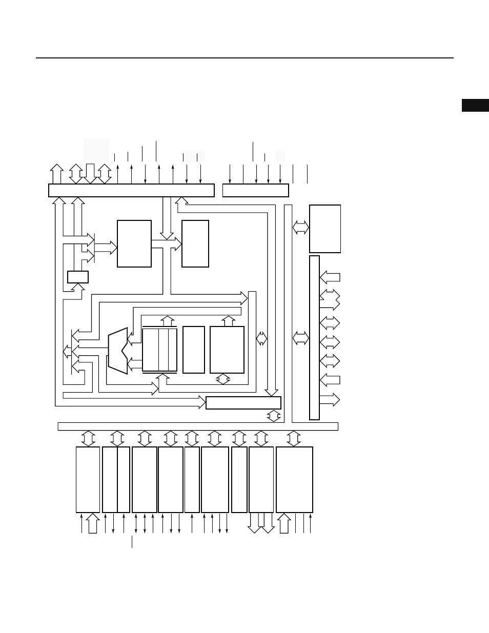
1.5 BLOCK DIAGRAM
Notes
1.
None for
µ
PD78213 and
µ
PD78213(A), 8KB for
µ
PD78212 and
µ
PD78212(A), 16KB for
µ
PD78214,
µ
PD78P214,
µ
PD78214(A)
2.
Internal dual-port RAM
3.
Peripheral RAM (PRAM). 128 bytes for
µ
PD78212 and
µ
PD78212(A), 256 bytes for
µ
PD78213,
µ
PD78214,
µ
PD78P214,
µ
PD78213(A),
and
µ
PD78214(A)
4.
For the
µ
PD78213, P40-P47, P50-P57, P64, or P65 do not operate as ports.
A16-A19 (expansion)
A8-A15
AD0-AD7
RD
WR
WAIT
REFRQ
ASTB
X1
X2
RESET
EA
V
DD
V
SS
System control
Bus control
• Micro ROM
• Micro-
sequencer
ROM
Note 1
PC
Address bus
ALU
Data bus
Bus interface
• RAM
(256 bytes)
Note 2
• GR
• Macro service
channel
Boolean
processpr
P70
-P75
P64
-P67
P60
-P63
P50
-P57
P40
-P47
P30
-P37
P20
-P27
P00
-P07
Port
RAM
Note 3
Temporary
registers
SP
PSW
Data bus (8)
NMI
INTP0-INTP5
R
X
D
T
X
D
ASCK
Programmable
interrupt controller
SCK
SO/SB0
SI
INTP3
TO0
TO1
INTP0
INTP1
INTP2
TO2
TO3
AN0-AN7
P00-P03
P04-P07
AVR
EF
AV
SS
INTP5
UART
Baud rate generator
Clocked serial interface
Timer/counter (16 bits)
Timer/counter
channel-1(PS+8 bits)
Timer/counter
channel-2 (PS+8 bits)
Timer/counter
channel-3 (PS+8 bits)
Real-time output port
(4 bits
×
2)
A/D converter
Shaded portions: In PROM
programming mode
General register
GR :
SFR address/data bus
P0
P2
P3
P4
P5
P6
P7
Note 4
Note 4
Note 4
A0-A14
D0-D7
CE
OE
V
PP