7 port 6 – NEC PD78214 User Manual
Page 113
84
µ
PD78214 Sub-Series
5.7 PORT 6
Port 6 is an 8-bit I/O port with an output latch. P64 through P67 have a software-programmable built-in pull-up
resistor.
In addition to the port functions, port 5 works as I/O pins for various control signals as listed in Table 5-7. Each
control pin is operated by the corresponding function.
For the
µPD78213, P64 and P65 function only as RD and WR output pins, respectively.
When the RESET signal is input, P60 through P63 go low, and P64 through P67 are put in the input port mode (high
output impedance state). At the same time, the contents of the higher 4 bits of the output latch become undefined,
and the lower 4 bits are reset to 0H.
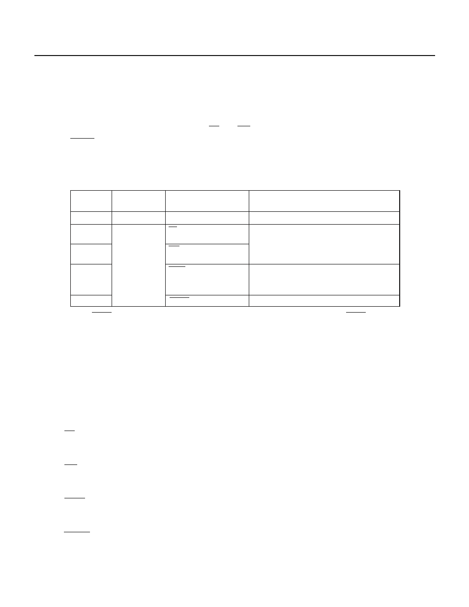
Table 5-7 Port 6 Operating Modes
P60-P63
P64
P66
P67
Output port
Set the MM6 bit of the MM register to 1.
For the
µPD78213, no special operation is
needed. For the other models, specify the
memory expansion mode by the MM2 through
MM0 bits of the MM register.
Specified by the PW register, or the PWn1 and
PWn0 bits (n = 2 or 3) of the MM register or by
putting P66 in the input mode.
Set the RFEN bit of the RFM register to 1.
Operation needed to make the pin function as a
control signal
A16-A19 output
RD output
WAIT input/AN6 input
REFRQ output/AN7 input
WR output
P65
I/O port
Pin
Control signal I/O mode
Port mode
Caution When the RESET signal exists, P60 through P63 are kept in the high impedance state. When the RESET signal disappears, they
output a low level. So, it is necessary to design the external circuit so that P60 through P63 are allowed to output a low level during
the initial state.
Remark See Chapter 13 for details.
(a) Port mode
P60 through P63 are output-only circuits. Each of P64 through P67 can be specified to be in either the input
or output mode by the port 6 mode register (PM6), independently of the other bits.
(b) Control signal I/O mode
(i) A16 through A19 (address bus)
These pins function as the upper address bus output pins when the external memory space is expanded
(10000H through FFFFFH). They operate according to the setting of the memory expansion register (MM).
(ii) RD (read strobe)
This pin outputs a strobe signal to read from external memory. For the
µPD78213, it always operates. For
the other models, it operates when the external memory is expanded.
(iii) WR (write strobe)
This pin outputs a strobe signal to write to external memory. For the
µPD78213, it always operates. For
the other models, it operates according to the setting of the MM register.
(iv) WAIT (wait)
This pin receives a wait signal. It operates according to the setting of the programmable wait control (PW)
register or the MM register.
(v) REFRQ (refresh request)
When a pseudo-static memory is connected to externally, this pin outputs a refresh pulse to the pseudo-
static memory. It operates according to the setting of the refresh mode register (RFM).