4 example of connecting pseudo static ram, 6 notes – NEC PD78214 User Manual
Page 401

372
µ
PD78214 Sub-Series
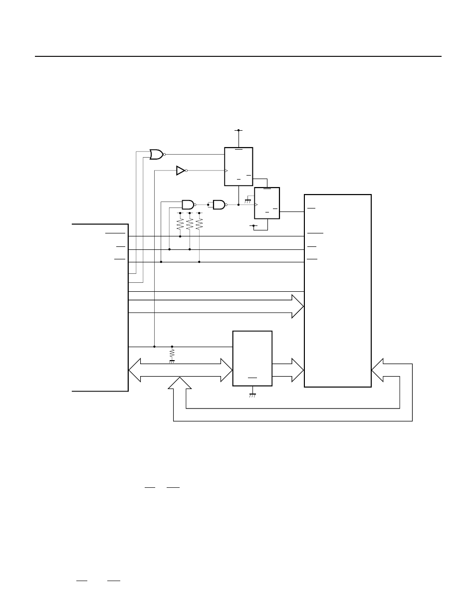
13.5.4 Example of Connecting Pseudo Static RAM
Fig. 13-23 shows an example of connecting pseudo static RAM to the
µPD78214. In this example, pseudo static
RAM is assigned to addresses 20000H to 3FFFFH.
Fig. 13-23 Example of Connecting Pseudo Static RAM to
µPD78214
Remarks
1. To ensure the precharge and access times for pseudo static RAM, devices of a sufficiently high speed must be used for those
devices identified as 74AC
××. To satisfy the precharge time for pseudo static RAM, use a high-speed product.
2. Pull-up resistors must be connected to the address and address/data bus lines.
13.6 NOTES
(1) Address information output on P50/A8 to P57/A15 and on P60/A16 to P63/A19 is valid from when the ASTB
signal goes high until the RD or WR signal goes high. Except during this period, the output levels of P50/A8
to P57/A15 and of P60/A16 to P63/A19 are undefined. When designing circuits, take this into consideration,
and make sure that the output of an undefined value will not cause any problems.
The data sheet of the relevant product gives the specification of the valid period for address output.
(2) External devices cannot be mapped onto the same addresses as those of the internal RAM area (
µPD78213,
µPD78214, and µPD78P214: 0FD00H to 0FEFFH, µPD78212: 0FD80H to 0FEFFH) and SFR area (0FF00H to
0FFFFH, excluding the external SFR area (0FF00H to 0FFDFH)).
Upon manipulating the space where external device addresses overlap with internal RAM or SFR addresses,
the internal RAM or SFR area is accessed automatically. In this case, the address signal is output, but the
ASTB, RD, and WR signals are not output (these signals remain inactive).
RFSH
REFRQ
OE
RD
WE
WR
CS
A17
LE
ASTB
A8-A16
A8-A16
A0-A7
A0-A7
CK
D
PR
R
Q
PR
R
CK
D
Q
CE
Pseudo-static RAM
V
DD
74AC74
74AC74
V
DD
74AC00
74AC00
74HC04
74HC02
OE
D0-D7 Q0-Q7
I/O1/-I/O8
74HC573
PD78214
µ
A18
A19
