Chapter 1 general – NEC PD78214 User Manual
Page 50

21
Chapter 1 General
1
Series name
µPD78214 Sub-Series
µPD78218A Sub-Series
µPD78214
µPD78214(A)
µPD78218A
Product
µPD78212
µPD78212(A)
µPD78213
µPD78213(A)
µPD78P214
µPD78P214(A) µ
PD78217A
µPD78P218A
Minimum instruction cycle
(when operating at 12 MHz)
333 ns
500 ns
333 ns
333 ns
500 ns
Operating voltage range
ROM
RAM
ROM-less
16K bytes
(masked ROM)
ROM-less
Internal memory
8K bytes
(masked ROM)
16K bytes
(PROM)
32K bytes
(masked ROM)
32K bytes
(PROM)
V
DD
= +5 V
±10%
512 bytes
1024 bytes
384 bytes
Number of I/O pins
54
36
54
54
36
Execution time (number of
clocks) required for PUSH
PSW instruction
• Five or seven when internal dual-port RAM is
used for the stack area
• Seven or nine in all other cases
• Six when internal dual-port RAM
is used for the stack area
• Eight in all other cases
One-shot output of 16-bit
timer/counter
Bit width of macro-service
counter
MPD or MPT increment in
macro-service type C
Restriction imposed on data
transfer from memory to SFR
in macro-service type A
Macro-service execution time
None
Supported
Eight bits
Eight bits or 16 bits (selectable,
except for macro service type A)
Only the eight lower-order bits are incremented.
(The eight high-order bits remain as is.)
The 16 bits are incremented.
Transfer data shall not be D0H to DFH.
Transfer source buffer (memory)
addresses shall not be 0FED0H to
0FEDFH.
The macro-service execution time depends on the macro-service mode and other
factors, and also varies with the sub-series. For details, refer to the table of macro-
service execution times in the relevant user's manual.
Restriction imposed
on input voltage
Restriction imposed
on the AV
REF
voltage
A voltage ranging from 0 V to AV
REF
can be
applied only to those pins for which A/D conver-
sion is performed and the pins selected by the
ANI0 to ANI3 bits of the ADM register.
A voltage ranging from 0 V to
AV
REF
can be applied only to those
pins for which A/D conversion is
being performed.
A/D converter
3.4 V to V
DD
3.6 V to V
DD
Oscillation settling time when
STOP mode is released
Pulse width of NMI at its active level, plus 16
counts on the corresponding counter
15 counts on the corresponding
counter or pulse width of NMI at its
active level, plus 16 counts on the
corresponding counter
• 64-pin plastic shrink DIP (750 mil) for all
products
• 64-pin plastic QUIP for all products other than
µPD78212, µPD78212(A), and µPD78P214(A)
• 68-pin plastic QFJ for all products other than
µPD78212, µPD78212(A), µPD78213(A), and
µPD78P214(A)
• 64-pin plastic QFP (14
× 14 mm) for all products
other than
µPD78213(A)
• 74-pin plastic QFP (20
× 20 mm) for all products
other than
µPD78212(A), µPD78213(A), and
µPD78P214(A)
• 64-pin ceramic shrink DIP with window (750
mil) for
µPD78P214 only
• 64-pin plastic shrink DIP (750 mil)
for all products
• 64-pin plastic QFP (14
× 14 mm)
for all products
• 64-pin ceramic shrink DIP with
window (750 mil) for the
µPD78P218A only
Package
V
DD
= +5 V
±0.3 V
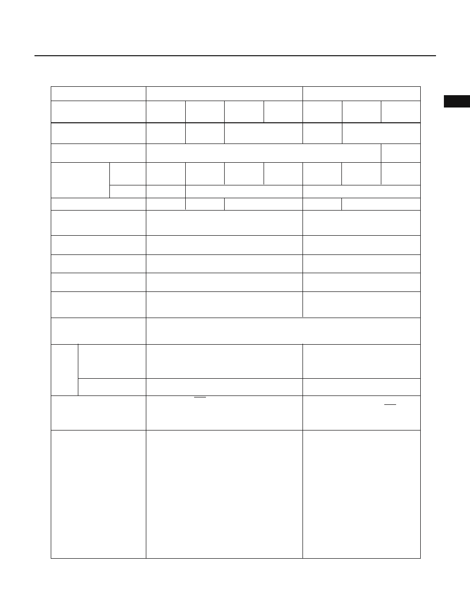
1.8 DIFFERENCES BETWEEN THE
µPD78214 SUB-SERIES AND µPD78218A SUB-SERIES
