2 configuration of the serial interface – NEC PD78214 User Manual
Page 299
270
µ
PD78214 Sub-Series
10.5.2 Configuration of the Serial Interface
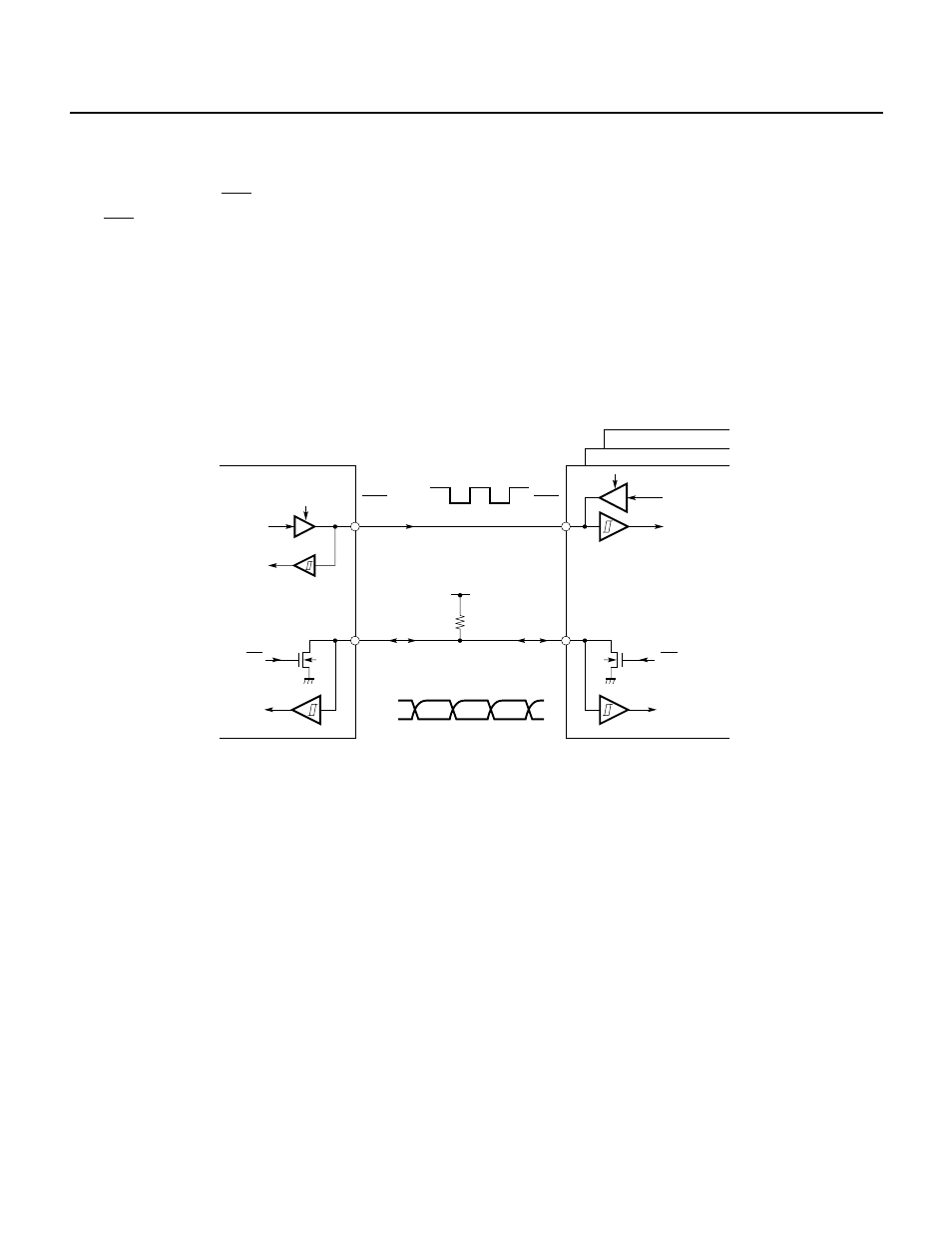
Fig. 10-9 is a block diagram of the
µPD78214.
The serial clock pin (SCK) and serial data bus pin SB0 are configured as shown in Fig. 10-8.
(1) SCK: Pin to input/output the serial clock
• Master : CMOS push-pull output
• Slave : Schmitt input
(2) SB0: Input/output pin for serial data
For both master and slave, N-ch open-drain output or Schmitt input
The serial data bus line requires an external pull-up resistor because of the N-ch open-drain output pin.
Fig. 10-8 Pin Configuration
SO
R
L
SI
SO
SI
SB0
SB0
Serial data bus
N-ch open-drain
N-ch open-drain
(Clock input)
Clock output
Clock input
(Clock output)
SCK
SCK
Serial clock
Master device
Slave device