3 memory mapping with expanded memory – NEC PD78214 User Manual
Page 379
350
µ
PD78214 Sub-Series
13.2.3 Memory Mapping with Expanded Memory
Figs. 13-6 to 13-9 show the memory maps when the memory has been expanded. Even when the memory has
been expanded, external devices at the same addresses as those of the internal ROM area, internal RAM area, or
SFR area (excluding the external SFR area (0FFD0H to 0FFDFH)) cannot be accessed. When these addresses are
accessed, the memory and SFRs of the
µPD78214 take precedence and are accessed. The ASTB, RD, and WR
signals are not output (these signals remain inactive). The output levels of the address bus and address/data bus
become undefined. However, when the memory is expanded, and the same execution cycle as the external ROM
fetch cycle is specified for internal ROM fetching (by setting the IFCH bit of the memory expansion mode register
(MM) to 0), the address signal and ASTB and RD signals are output upon access to internal ROM. Information on
the address/data bus at this time, however, is not read, and the CPU reads data from internal ROM. (When the RD
signal is active, the address/data bus of the
µPD78214 becomes high-impedance.)
The bus cycle in this case is the same as the normal read cycle. So, the programmable wait function can insert
wait states into the bus cycle.
Caution When macro service Type A or Type C is used in external memory expansion mode (the
µPD78213 always uses external memory),
an illegal write access may occur. This occurs when any of the following three conditions is satisfied:
(1) Data is transferred from memory to an SFR using macro service Type A, and the transfer data is D0H to DFH.
(2) Data is transferred from an SFR to memory using macro service Type A, and the transfer destination buffer (memory) address
is 0FED0H to 0FEDFH when the macro service is executed.
(3) The MPTL address is 0FED0H to 0FEDFH when macro service Type C is used.
An illegal write access is performed in the same way as normal memory access. In addition, wait states are inserted according to
the setting of bits PW20 and PW21 of the memory expansion mode register (MM). Table 13-1 lists the conditions and operations
for illegal write access.
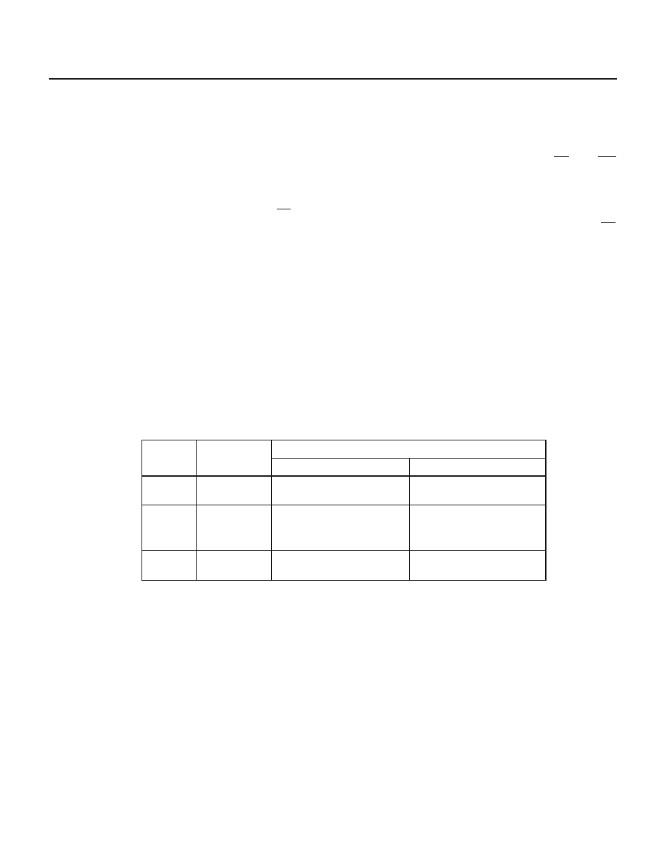
Table 13-1 Conditions and Operations for Illegal Write Access
Condition
Macro service
type
1
2
3
A
A
C
Illegal write access
Data
Data transferred by macro
service
Low-order 8 bits of transfer
destination buffer (memory)
address
Low-order 8 bits of MPTL
address
This problem can be avoided by using the following methods:
1. The problem caused by condition 1 is difficult to avoid by means of software (because whether an illegal access occurs depends
on the transfer data). The problem must be avoided by using the external address decoder so that the area at addresses 0FF00H
to 0FFFFH does not overlap the addresses of the external circuits.
2. When the macro service being used does not satisfy condition 1 (transfer from memory to an SFR is not performed by macro
service Type A), or when condition 2 is satisfied, the buffer area must be mapped to an address other than addresses 0FED0H
to 0FEDFH. In the case of condition 3, the MPTL must be mapped to an address other than addresses 0FED0H to 0FEDFH.
This problem can also occur in the in-circuit emulator.
Address
Transfer destination SFR
address
Transfer destination SFR
(CR10 or CR11) address
Transfer target SFR address