NEC PD78214 User Manual
Page 419
390
µ
PD78214 Sub-Series
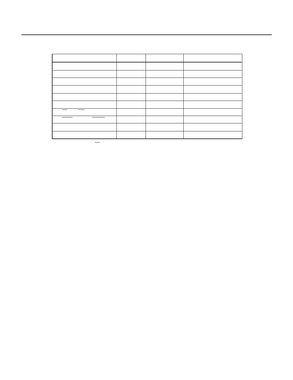
Table 15-1 Pin States during Reset and After Reset State Is Released
Pin name
P00-P07
P20/NMI-27/SI
P30/RxD-P37/TO3
P40/AD0-P47/AD7
P50/A8-P57/A15
P60/A16-P63/A19
P64/RD, P65/WR
P66/WAIT/AN6, P67/REFRQ/AN7
P70/AN0-P75/AN5
ASTB
I/O
Output
Input
I/O
I/O
I/O
Output
I/O
I/O
Input
Output
During reset
Hi-Z
Hi-Z
Hi-Z
Hi-Z
Hi-Z
Hi-Z
Hi-Z
Hi-Z
Hi-Z
Hi-Z
After reset state is released
Hi-Z
Hi-Z (input port)
Hi-Z (input port mode)
Hi-Z (input port mode)
Note
Hi-Z (input port mode)
Note
0
Hi-Z (input port mode)
Note
Hi-Z (input port mode)
Hi-Z (input port mode)
0
Note When ROM-less mode is specified (EA pin = 0), these pins function as an address/data bus and output signals for fetching the reset vector
address from address 0000H (see Fig. 15-3 (a)).