7 gpio interface signals, Table 3.7 scsi gpio function a signals, Gpio interface signals – Avago Technologies LSI53C876E User Manual
Page 83: Scsi gpio function a signals
PCI Interface Signals
3-11
3.1.7 GPIO Interface Signals
describes the signals for the SCSI GPIO Function A Signals
group.
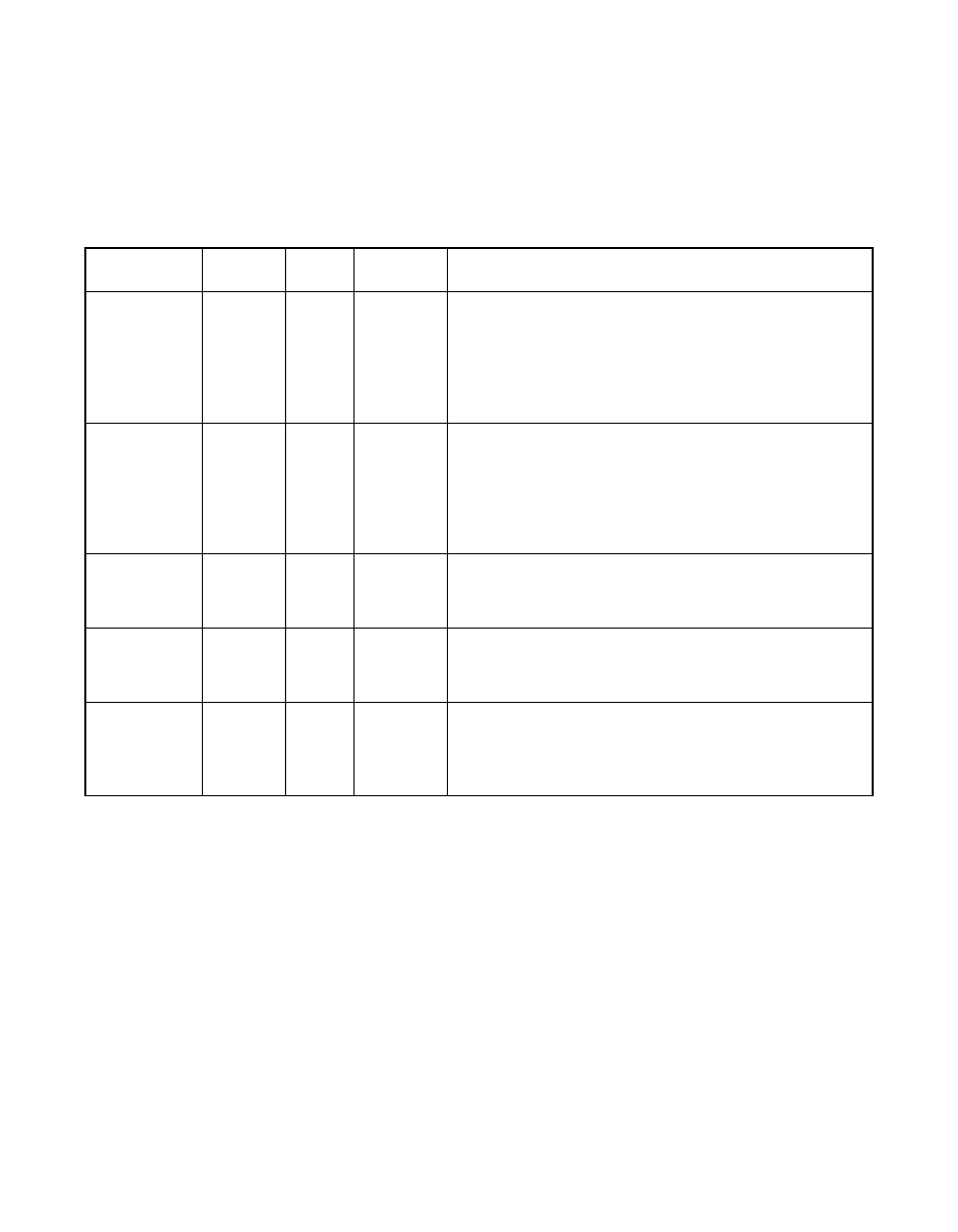
Table 3.7
SCSI GPIO Function A Signals
Name
Pin No.
Type
Strength
Description
A_GPIO0_
FETCH/
68, W7
I/O
16 mA
SCSI Function A General Purpose I/O pin 0.
Optionally, when driven LOW, indicates that the next
bus request is for an opcode fetch. This pin is
programmable at power-up through the MAD[7:6] pins
to serve as either the data or clock signal for the serial
EEPROM interface.
A_GPIO1_
MASTER/
69, Y7
I/O
16 mA
SCSI Function A General Purpose I/O pin 1.
Optionally, when driven LOW, indicates that the
LSI53C876 is bus master. This pin is programmable
at power-up through the MAD[7:6] pins to serve as
either the data or clock signal for the serial EEPROM
interface.
A_GPIO2
70, V8
I/O
16 mA
SCSI Function A General Purpose I/O pin 2. This
pin is a general purpose I/O pin that powers up as an
input.
A_GPIO3
71, W8
I/O
16 mA
SCSI Function A General Purpose I/O pin 3.
A_GPIO3 powers up as an input. Currently our drivers
use A_GPIO3 as a means to detect Diffsense.
A_GPIO4
73, Y8
I/O
16 mA
SCSI Function A General Purpose I/O pin 4.
A_GPIO4 powers up as an output. It can be used as
the enable line for VPP, the 12 V power supply to the
external Flash memory interface.