Figure5.2 block move instruction register, Block move instruction register – Avago Technologies LSI53C876E User Manual
Page 198
5-8
SCSI SCRIPTS Instruction Set
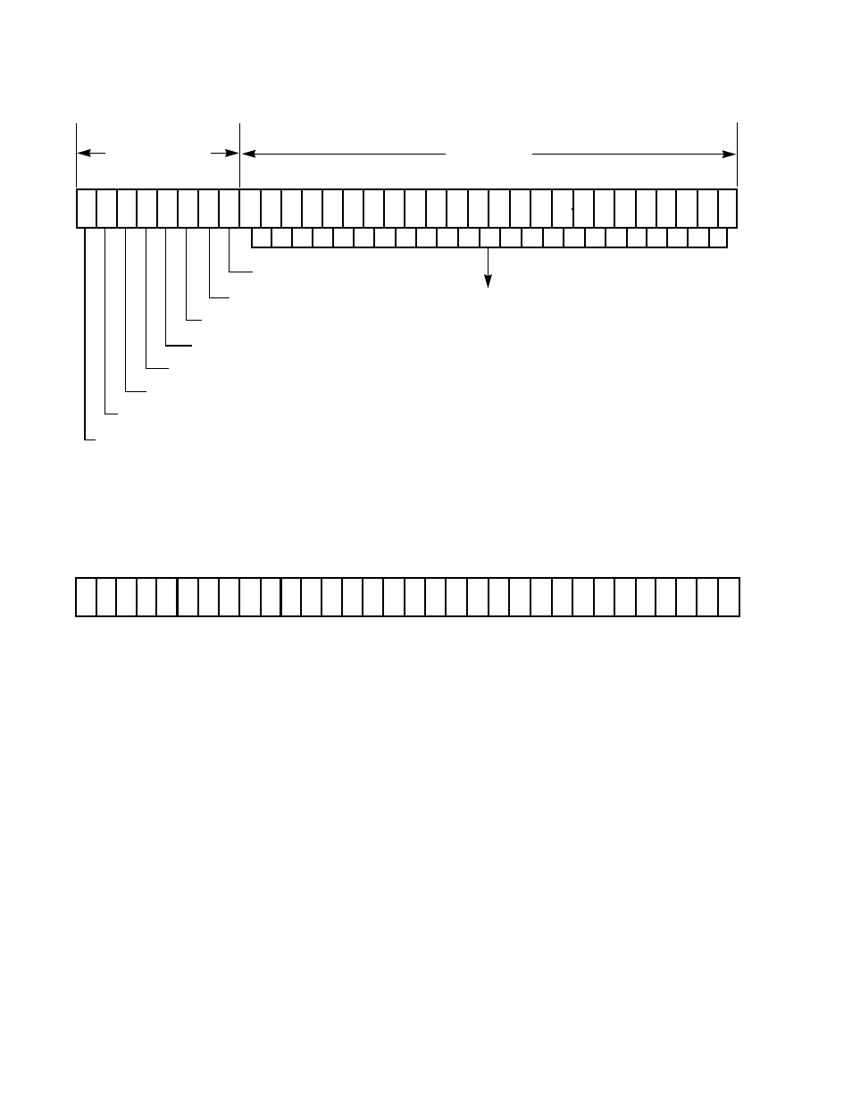
Figure 5.2
Block Move Instruction Register
Prior to the start of an I/O, load the
with the base address of the I/O data
structure. Any address on a long word boundary is
allowed.
After a Table Indirect opcode is fetched, the DSA is
added to the 24-bit signed offset value from the opcode
to generate the address of the required data; both
positive and negative offsets are allowed. A subsequent
fetch from that address brings the data values into the
chip.
For a MOVE instruction, the 24-bit byte count is fetched
from system memory. Then the 32-bit physical address is
brought into the LSI53C876. Execution of the move
begins at this point.
31 30 29 28 27 26 25 24 23 22 21 20 19 18 17 16 15 14 13 12 11 10 9
8
7
6
5
4
3
2
1
0
31 30 29 28 27 26 25 24 23 22 21 20 19 18 17 16 15 14 13 12 11 10 9
8
7
6
5
4
3
2
1
0
DSPS Register
DCMD Register
DBC Register
24-Bit Block Move Byte Counter
I/O
C/D
MSG/
Opcode
Table Indirect Addressing
Indirect Addressing (LSI53C700 Family Compatible)
0 - Instruction Type - Block Move
0 - Instruction Type - Block Move