Chip test three (ctest3), Chip test three, Ctest3) – Avago Technologies LSI53C876E User Manual
Page 150: Register: 0x1b
4-56
Registers
DACK
Data Acknowledge Status
0
This bit indicates the status of the LSI53C876 SCSI
function’s internal Data Acknowledge signal (DACK/).
When this bit is set, DACK/ is inactive. When this bit is
clear, DACK/ is active.
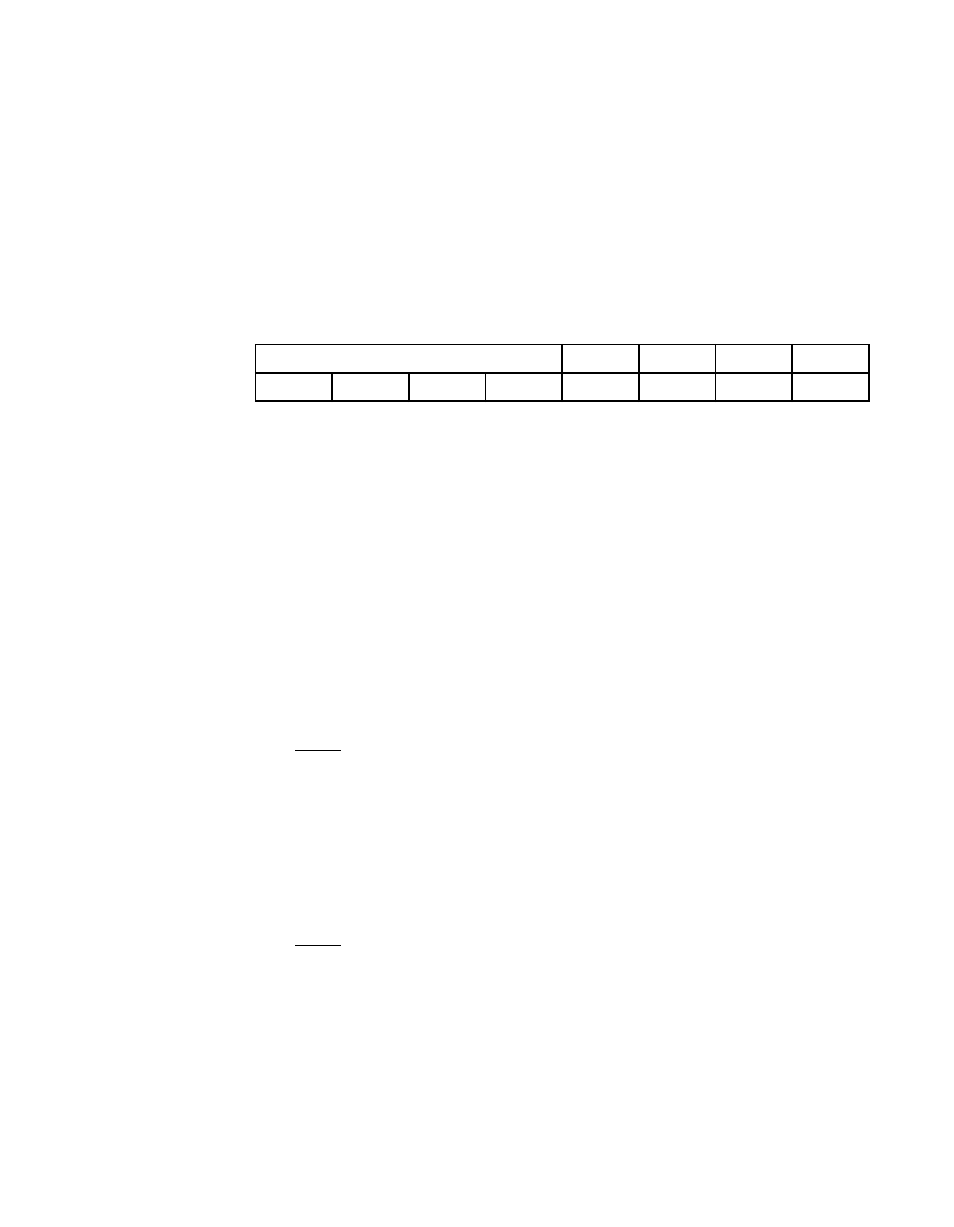
Register: 0x1B
Chip Test Three (CTEST3)
Read/Write
V[3:0]
Chip Revision Level
[7:4]
These bits identify the chip revision level for software
purposes. It should have the same value as the lower
nibble of the PCI
register.
FLF
Flush DMA FIFO
3
When this bit is set, data residing in the DMA FIFO is
transferred to memory, starting at the address in the
register. The internal DMAWR
signal, controlled by the
register, determines the direction of the transfer. This bit
is not self-clearing; clear it once the data is successfully
transferred by the LSI53C876 SCSI function.
Note:
Polling of FIFO flags is allowed during flush operations.
CLF
Clear DMA FIFO
2
When this bit is set, all data pointers for the DMA FIFO
are cleared. Any data in the FIFO is lost. After the
LSI53C876 SCSI function successfully clears the
appropriate FIFO pointers and registers, this bit
automatically clears.
Note:
This bit does not clear the data visible at the bottom of the
FIFO.
7
4
3
2
1
0
V[3:0]
FLF
CLF
FM
WRIE
x
x
x
x
0
0
0
0