1 3.3 v pci timings, Table 6.24 3.3 v pci timing, 3 v pci timing – Avago Technologies LSI53C876E User Manual
Page 248
6-16
Electrical Characteristics
•
Read Cycle, Normal/Fast Memory (
•
Write Cycle, Normal/Fast Memory (
•
•
•
•
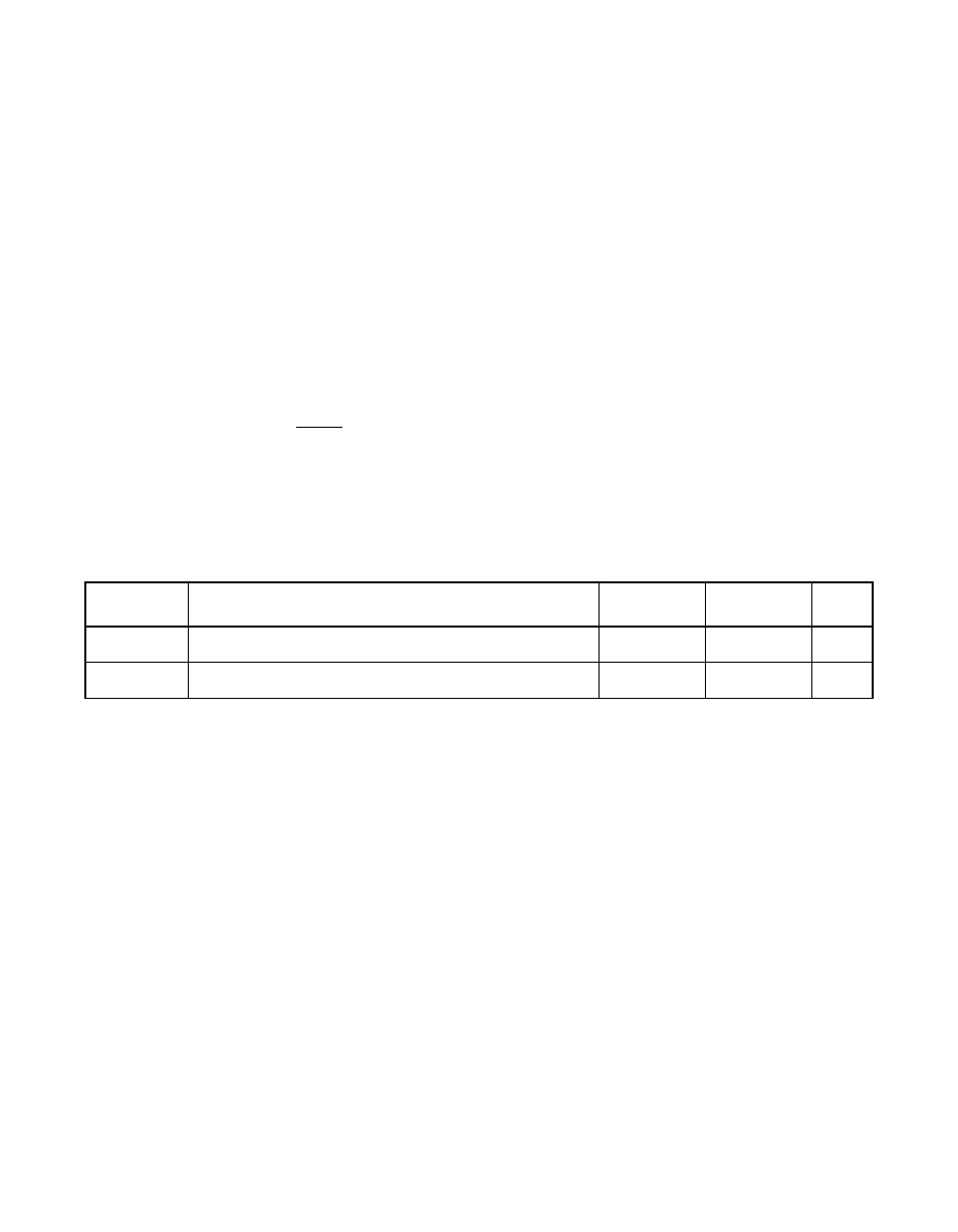
6.4.1.1 3.3 V PCI Timings
Note:
When a 3.3 V source is applied to the V
DD
-I pins of the
LSI53C876, some of the PCI timing data in
through
will change. The 3.3 V PCI timing data
is listed in
Table 6.24
3.3 V PCI Timing
Symbol
Parameter
Min
Max
Unit
t
2
Shared signal input hold time
1
–
ns
t
3
CLK to shared signal output valid
–
12
ns
See also other documents in the category Avago Technologies Hardware:
- MGA-725M4 (4 pages)
- MGA-71543 (4 pages)
- MGA-71543 (3 pages)
- MGA-82563 (6 pages)
- 3ware SAS 9750-8i (48 pages)
- 3ware 9690SA-8I (Channel) (138 pages)
- 3ware 9690SA-8I (Channel) (380 pages)
- 3ware SAS 9750-8i (29 pages)
- 3ware 9550SXU-8LP (Channel) (149 pages)
- 3ware 9550SXU-8LP (Channel) (40 pages)
- 3ware 9650SE-8LPML (Channel) (45 pages)
- 3ware 9690SA-8I (Channel) (361 pages)
- 3ware 9690SA-8I (Channel) (27 pages)
- 6160 SAS Switch (2 pages)
- MegaRAID SAS 9361-8i (13 pages)
- MegaRAID SAS 9266-8i (12 pages)
- MegaRAID SAS 9380-8e (43 pages)
- Cache Protection for RAID Controller Cards (139 pages)
- Cache Protection for RAID Controller Cards (13 pages)
- MegaRAID SAS 9271-8iCC (13 pages)
- MegaRAID SAS 9285-8ecv (92 pages)
- MegaRAID SAS 9266-8i (20 pages)
- MegaRAID SAS 9271-8iCC (26 pages)
- MegaRAID SafeStore Software (502 pages)
- MegaRAID SAS 9285-8ecv (80 pages)
- MegaRAID SAS 0260CV-4i (64 pages)
- MegaRAID SAS 0260CV-4i (49 pages)
- MegaRAID SAS 9271-8i (8 pages)
- MegaRAID SAS 0260CV-4i (72 pages)
- MegaRAID SAS 9361-8i (7 pages)
- MegaRAID SAS 9341-8i (8 pages)
- MegaRAID SAS 9380-4i4e (7 pages)
- MegaRAID SAS 9380-8e (7 pages)
- MegaRAID SAS 9240-8i (4 pages)
- MegaRAID SAS 0260CV-4i (28 pages)
- MegaRAID SAS 9260-16i (12 pages)
- MegaRAID SAS 9280-24i4e (14 pages)
- MegaRAID SAS 9280-24i4e (16 pages)
- MegaRAID SAS 9260-8i (4 pages)
- MegaRAID SafeStore Software (8 pages)
- MegaRAID SAS 9280-8e (22 pages)
- MegaRAID SAS 9261-8i (4 pages)
- MegaRAID SAS 9285-8e (12 pages)
- MegaRAID SAS 9280-16i4e (12 pages)
- MegaRAID SAS 9280-4i4e (4 pages)