Figure2.2 parity checking/generation, 6 dma fifo, Figure2.3 dma fifo sections – Avago Technologies LSI53C876E User Manual
Page 42: Dma fifo, Parity checking/generation, Dma fifo sections, Figure 2.2
2-20
Functional Description
Figure 2.2
Parity Checking/Generation
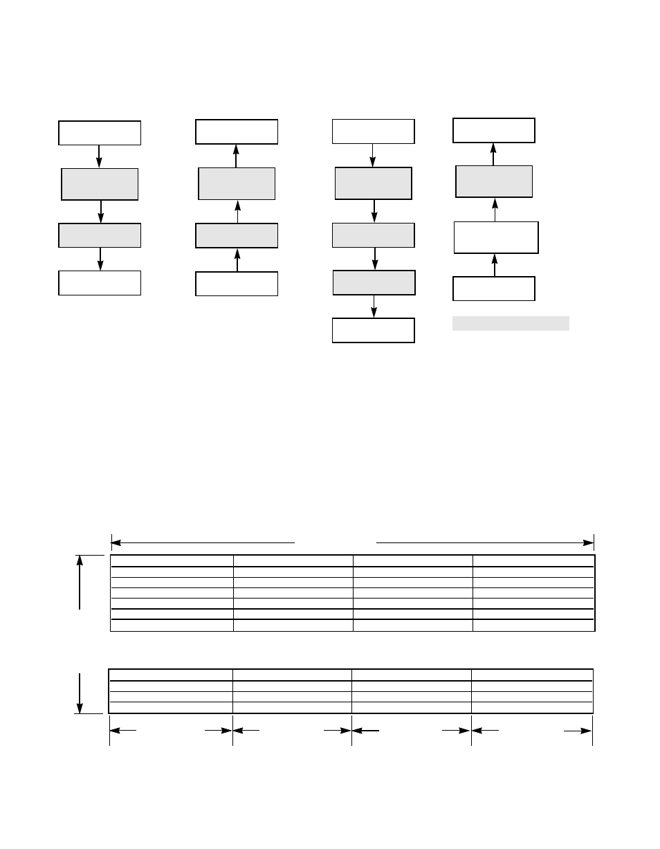
2.2.6 DMA FIFO
The DMA FIFO is 4 bytes wide by 134 transfers deep. The DMA FIFO is
illustrated in
. The default DMA FIFO size is 88 bytes to assure
compatibility with older products in the LSI53C8XX family.
The DMA FIFO size may be set to 536 bytes by setting the DMA FIFO
Size bit, bit 5, in the
register.
Figure 2.3
DMA FIFO Sections
PCI Interface**
DMA FIFO*
(32 Bits x 134)
SODL Register*
SCSI Interface**
X
S
PCI Interface**
DMA FIFO*
(32 Bits x 134)
SIDL Register*
SCSI Interface**
G
X
PCI Interface**
DMA FIFO*
(32 Bits x 134)
SODL Register*
SCSI Interface**
X
S
SODR Register*
PCI Interface**
DMA FIFO*
(32 Bits x 134)
SCSI Interface**
G
X
SCSI FIFO*
(8 or 16 Bits x 16)
X
* = No parity protection
** = Parity protected
Asynchronous
SCSI Send
Asynchronous
SCSI Receive
Synchronous
SCSI Send
Synchronous
SCSI Receive
X - Check parity
G - Generate 32-bit even PCI parity
S - Generate 8-bit odd SCSI parity
134
Transfers
Deep
.
.
.
32 Bytes Wide
8 Bits
Byte Lane 3
8 Bits
Byte Lane 2
8 Bits
Byte Lane 1
8 Bits
Byte Lane 0
134
Transfers
Deep
.
.
.
.
.
.
32 Bytes Wide
8 Bits
Byte Lane 3
8 Bits
Byte Lane 2
8 Bits
Byte Lane 1
8 Bits
Byte Lane 0