Dma mode (dmode), Dma mode, Dmode) – Avago Technologies LSI53C876E User Manual
Page 160: Scratch register a, Scratcha), Scratch register a (scratcha), Register: 0x34, Register: 0x38

4-66
Registers
Register: 0x34
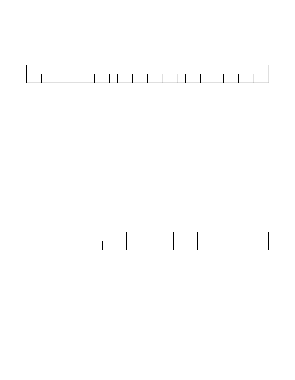
Scratch Register A (SCRATCHA)
Read/Write
SCRATCHA
Scratch Register A
[31:0]
This is a general purpose, user-definable scratch pad
register. Apart from CPU access, only Register
Read/Write and Memory Moves into the SCRATCH
register alter its contents. The power-up value of this
register is indeterminate.
A special mode of this register is enabled by setting the
BAE bit in the
register. If this bit
is set, the
register
returns the memory base address of the chip registers on
the upper 24 bits of the data bus when the SCRATCHA
register is read. Writes to the SCRATCHA register are
unaffected. Resetting the BAE bit causes the SCRATCHA
register to return to normal operation.
Register: 0x38
DMA Mode (DMODE)
Read/Write
BL[1:0]
Burst Length
[7:6]
These bits control the maximum number of transfers
performed per bus ownership, regardless of whether the
transfers are back-to-back, burst, or a combination of
both. The LSI53C876 SCSI function asserts the Bus
Request (REQ/) output when the DMA FIFO can
accommodate a transfer of at least one burst size of data.
Bus Request (REQ/) is also asserted during start-of-
transfer and end-of-transfer cleanup and alignment, even
if less than a full burst of transfers is performed. The
LSI53C876 SCSI function inserts a “fairness delay” of
four CLKs between burst transfers (as set in BL[1:0])
31
0
SCRATCHA
x
x
x
x
x
x
x
x
x
x
x
x
x
x
x
x
x
x
x
x
x
x
x
x
x
x
x
x
x
x
x
x
7
6
5
4
3
2
1
0
BL[1:0]
SIOM
DIOM
ER
ERMP
BOF
MAN
0
0
0
0
0
0
0
0
