2 pci and external memory interface timing, Pci and external memory interface timing, Lsi53c876 pci and external memory interface timing – Avago Technologies LSI53C876E User Manual
Page 286
6-54
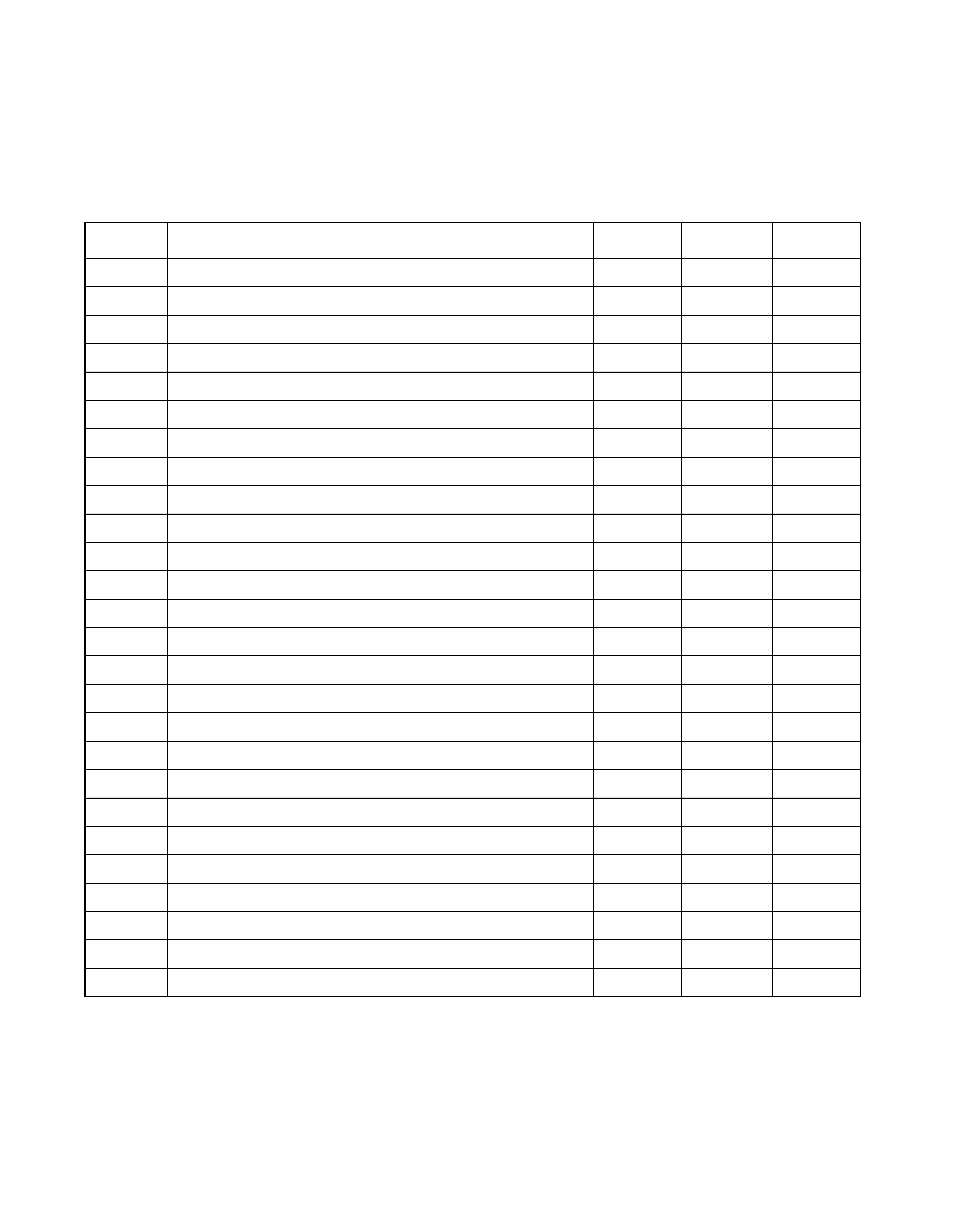
Electrical Characteristics
6.4.2 PCI and External Memory Interface Timing
lists the PCI and External Memory Interface timing data.
Table 6.42
LSI53C876 PCI and External Memory Interface Timing
Symbol
Parameter
Min
Max
Unit
t
1
Shared signal input setup time
7
–
ns
t
2
Shared signal input hold time
0
–
ns
t
3
CLK to shared signal output valid
–
11
ns
t
4
Side signal input setup time
10
–
ns
t
5
Side signal input hold time
0
–
ns
t
6
CLK to side signal output valid
–
12
ns
t
7
CLK high to FETCH/ low
–
20
ns
t
8
CLK high to FETCH/ high
–
20
ns
t
9
CLK high to MASTER/ low
–
20
ns
t
10
CLK high to MASTER/ high
–
20
ns
t
11
Address setup to MAS/ high
25
–
ns
t
12
Address hold from MAS/ high
15
–
ns
t
13
MAS/ pulse width
25
–
ns
t
14
MCE/ low to data clocked in
160
–
ns
t
15
Address valid to data clocked in
205
–
ns
t
16
MOE/ low to data clocked in
100
–
ns
t
17
Data hold from address, MOE/, MCE/ change
0
–
ns
t
18
Address out from MOE/, MCE/ high
50
–
ns
t
19
Data setup to CLK high
5
–
ns
t
20
Data setup to MWE/ low
30
–
ns
t
21
Data hold from MWE/ high
20
–
ns
t
22
MWE/ pulse width
100
–
ns
t
23
Address setup to MWE/ low
75
–
ns
t
24
MCE/ low to MWE/ high
120
–
ns
t
25
MCE/ low to MWE/ low
25
–
ns
t
26
MWE/ high to MCE/ high
25
–
ns