Table 2.7 mode a serial eeprom data format, 2 mode b operation, 3 mode c operation – Avago Technologies LSI53C876E User Manual
Page 68: Mode b operation, Mode c operation, Mode a serial eeprom data format, Table 2.7
2-46
Functional Description
2.4.2 Mode B Operation
A 4.7 K pull-down on MAD6, no pull-down on MAD7. In this mode,
GPIO0 and GPIO1 are each defined as either the SDA or the SCL, since
both pins are controlled through software.
No data is automatically loaded into chip registers at power-up or hard
reset. The
register and
register are
read/write, in violation of the PCI specification, with a default value of all
zero’s.
2.4.3 Mode C Operation
A 4.7 K pull-down on MAD6, and a 4.7 K pull-down on MAD7. In this
mode, GPIO1 is the SDA and GPIO0 is the SCL. Certain data in the
serial EEPROM is automatically loaded into chip registers at
power-up or hard reset.
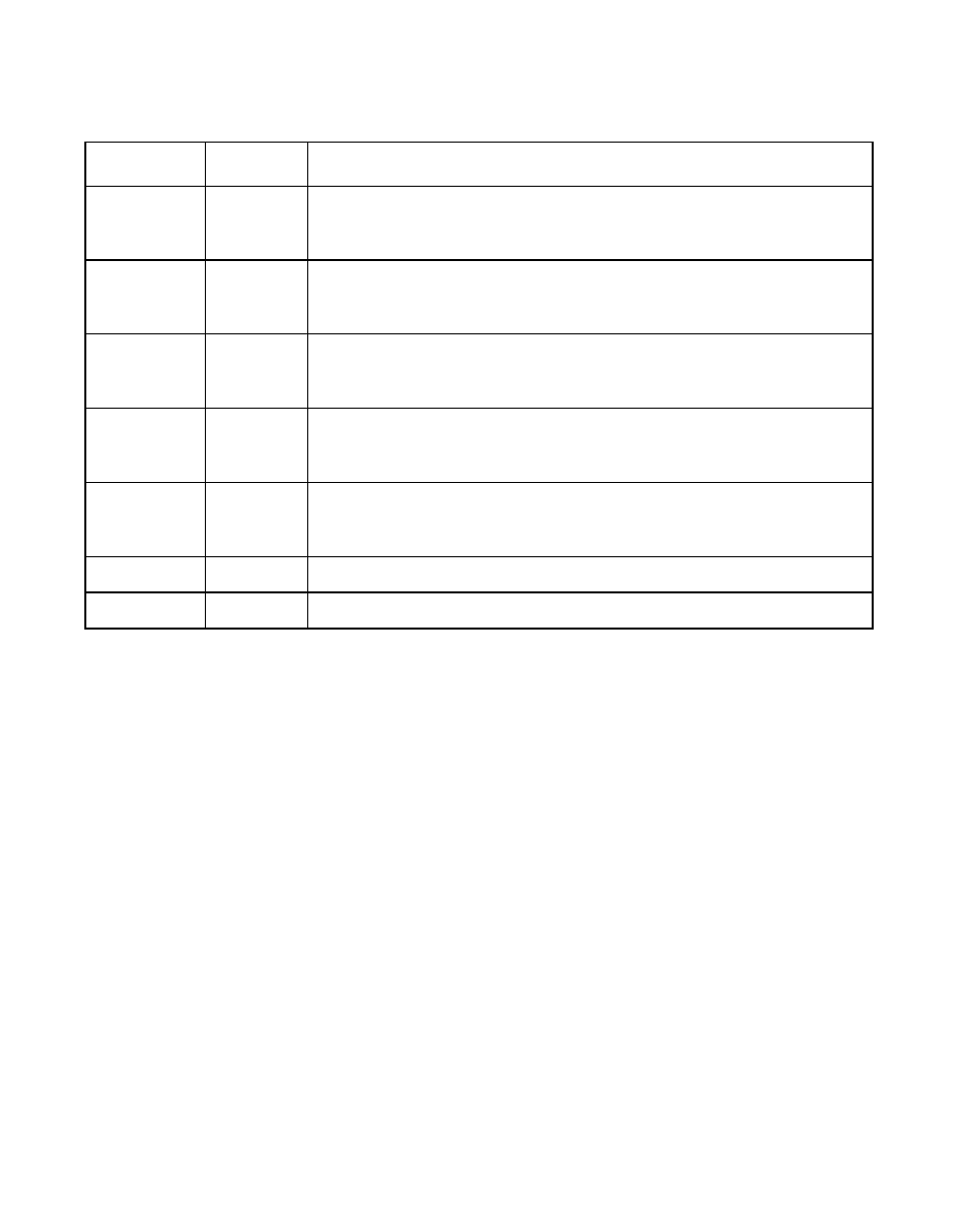
Table 2.7
Mode A Serial EEPROM Data Format
Byte
Name
Description
0x00
SVID(0)
, LSB. This byte is loaded into the least significant
byte of the
register in the appropriate PCI
configuration space at chip power-up or hard reset.
0x01
SVID(1)
, MSB. This byte is loaded into the most significant
byte of the
register in the appropriate PCI
configuration space at chip power-up or hard reset.
0x02
SID(0)
, LSB. This byte is loaded into the least significant byte of
the
register in the appropriate PCI configuration space at
chip power-up or hard reset.
0x03
SID(1)
, MSB. This byte is loaded into the most significant byte
of the
register in the appropriate PCI configuration space
at chip power-up or hard reset.
0x04
CKSUM
Checksum. This 8-bit checksum is formed by adding, bytewise, each
byte contained in locations 0x00–0x03 to the seed value 0x55, and then
taking the 2’s complement of the result.
0x05–0xFF
RSV
Reserved.
0x100–EOM
UD
User Data.