Chip test two (ctest2), Register: 0x19, Register: 0x1a – Avago Technologies LSI53C876E User Manual
Page 148

4-54
Registers
Register: 0x19
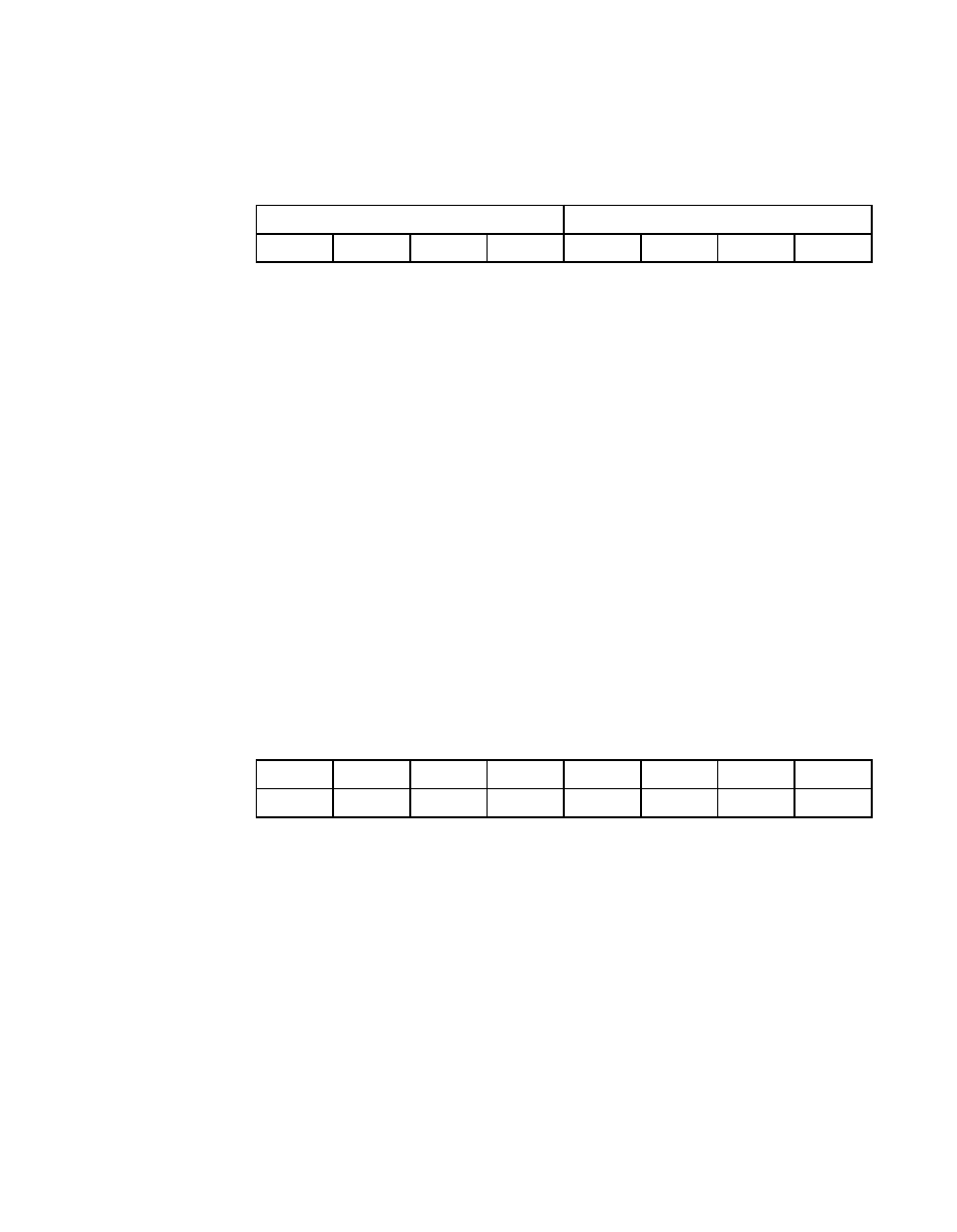
Chip Test One (CTEST1)
Read Only
FMT[3:0]
Byte Empty in DMA FIFO
[7:4]
These bits identify the bottom bytes in the DMA FIFO that
are empty. Each bit corresponds to a byte lane in the
DMA FIFO. For example, if byte lane three is empty, then
FMT3 is set. Since the FMT flags indicate the status of
bytes at the bottom of the FIFO, if all FMT bits are set,
the DMA FIFO is empty.
FFL[3:0]
Byte Full in DMA FIFO
[3:0]
These status bits identify the top bytes in the DMA FIFO
that are full. Each bit corresponds to a byte lane in the
DMA FIFO. For example, if byte lane three is full then
FFL3 is set. Since the FFL flags indicate the status of
bytes at the top of the FIFO, if all FFL bits are set, the
DMA FIFO is full.
Register: 0x1A
Chip Test Two (CTEST2)
Read Only
DDIR
Data Transfer Direction
7
This status bit indicates which direction data is being
transferred. When this bit is set, the data is transferred
from the SCSI bus to the host bus. When this bit is clear,
the data is transferred from the host bus to the SCSI bus.
SIGP
Signal Process
6
This bit is a copy of the SIGP bit in the
register (bit 5). The SIGP bit signals a running
SCRIPTS instruction. When this register is read, the
SIGP bit in the ISTAT register is cleared.
7
4
3
0
FMT[3:0]
FFL[3:0]
1
1
1
1
0
0
0
0
7
6
5
4
3
2
1
0
DDIR
SIGP
CIO
CM
SRTCH
TEOP
DREQ
DACK
0
0
x
x
0
0
0
1
