Altera Arria V Hard IP for PCI Express User Manual
Page 227
Chapter 17: Testbench and Design Example
17–5
Chaining DMA Design Examples
December 2013
Altera Corporation
Arria V Hard IP for PCI Express
User Guide
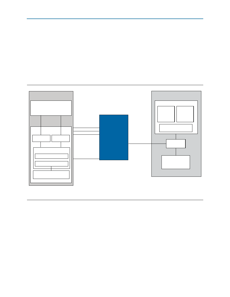
The BFM driver writes the descriptor tables into BFM shared memory, from which the
chaining DMA design engine continuously collects the descriptor tables for DMA
read, DMA write, or both. At the beginning of the transfer, the BFM programs the
Endpoint chaining DMA control register. The chaining DMA control register indicates
the total number of descriptor tables and the BFM shared memory address of the first
descriptor table. After programming the chaining DMA control register, the chaining
DMA engine continuously fetches descriptors from the BFM shared memory for both
DMA reads and DMA writes, and then performs the data transfer for each descriptor
shows a block diagram of the design example connected to an external
RC CPU.
The block diagram contains the following elements:
■
Endpoint DMA write and read requester modules.
Figure 17–2. Top-Level Chaining DMA Example for Simulation
Note to
(1) For a description of the DMA write and read registers, refer to
.
Root Complex
CPU
Root Port
Memory
Write
Descriptor
Table
Data
Chaining DMA
Endpoint Memory
Avalon-MM
interfaces
Hard IP for
PCI Express
DMA Control/Status Register
DMA Read
Avalon-ST
Configuration
PCI Express
DMA Write
DMA Wr Cntl (0x0-4)
DMA Rd Cntl (0x10-1C)
RC Slave
Read
Descriptor
Table