Altera Arria V Hard IP for PCI Express User Manual
Page 161
Chapter 8: Register Descriptions
8–7
Altera-Defined Vendor Specific Extended Capability (VSEC)
December 2013
Altera Corporation
Arria V Hard IP for PCI Express
User Guide
Table 8–15
defines the fields of the
CvP Status
register. This register allows software
to monitor the CvP status signals.
Table 8–16
defines the fields of the CvP Mode Control register which provides global
control of the CvP operation.
f
Refer to
for
more information about using CvP.
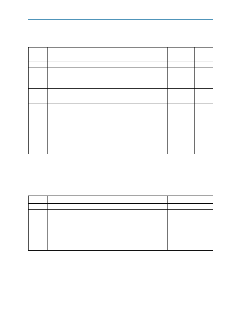
Table 8–15. CvP Status
Bits
Register Description
Reset Value
Access
[15:10]
Reserved.
0x00
RO
[9]
PLD_CORE_READY
. From FPGA fabric. This status bit is provided for debug.
Variable
RO
[8]
PLD_CLK_IN_USE
. From clock switch module to fabric. This status bit is
provided for debug.
Variable
RO
[7]
CVP_CONFIG_DONE
. Indicates that the FPGA control block has completed the
device configuration via CvP and there were no errors.
Variable
RO
[6]
CVP_HF_RATE_SEL
. Indicates if the FPGA control block interface to the Arria V
Hard IP for PCI Express is operating half the normal frequency–62.5MHz,
instead of full rate of 125MHz
Variable
RO
[5]
USERMODE
. Indicates if the configurable FPGA fabric is in user mode.
Variable
RO
[4]
CVP_EN
. Indicates if the FPGA control block has enabled CvP mode.
Variable
RO
[3]
CVP_CONFIG_ERROR
. Reflects the value of this signal from the FPGA control
block, checked by software to determine if there was an error during
configuration
Variable
RO
[2]
CVP_CONFIG_READY – reflects the value of this signal from the FPGA control
block, checked by software during programming algorithm
Variable
RO
[1]
Reserved.
—
—
[0]
Reserved.
—
—
Table 8–16. CvP Mode Control (Part 1 of 2)
Bits
Register Description
Reset Value
Access
[31:16]
Reserved. 0x0000
RO
[15:8]
CVP_NUMCLKS
. Specifies the number of CvP clock cycles required for every CvP
data register write. Valid values are 0x00–0x3F, where 0x00 corresponds to 64
cycles, and 0x01-0x3F corresponds to 1 to 63 clock cycles. The upper bits are
not used, but are included in this field because they belong to the same byte
enable.
0x00
RW
[7:4]
Reserved. 0x0
RO
[2]
CVP_FULLCONFIG
. Request that the FPGA control block reconfigure the entire
FPGA including the Arria V Hard IP for PCI Express, bring the PCIe link down.
1’b0
RW