4 95.85-mhz peripheral phase locked loop – Intel PXA26X User Manual
Page 71
Intel® PXA26x Processor Family Developer’s Manual
3-5
Clocks and Power Manager
3.3.4
95.85-MHz Peripheral Phase Locked Loop
The 95.85-MHz PLL is the clock source for many of the peripheral blocks’ external interfaces.
These interfaces require: ~48 MHz for the UDC/USB, fast infrared communications port (FICP),
~33 MHz for the I
2
C, and ~20 MHz for the MMC. The generated frequency is not exactly the
required frequency due to the chosen crystal and the lack of a perfect least common multiple
between the units. The chosen frequencies keep each unit’s clock frequency within the unit’s clock
tolerance. If a crystal other than 3.6864 MHz is used, the clock frequencies to the peripheral
blocks’ interfaces may not yield the desired baud rates (or protocol’s rate).
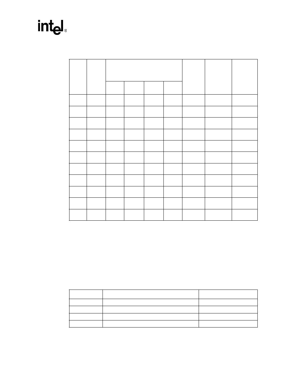
Table 3-1. Core PLL Output Frequencies for 3.6864-MHz Crystal
L
M
Turbo Mode Frequency (MHz) for Values
“N” and Core Clock
Configuration Register (CCCR[15:0])
programming for Values of “N”:
PXbus
Frequency
(MHz)
MEM, LCD
Frequency
(MHz)
SDRAM
max Freq
(MHz)
1.00
(Run)
1.50
2.00
3.00
27
1
99.5
@.85 V
—
199.1
@1.0 V
298.6
@1.1 V
50
99.5
99.5
32
1
118.0
@1.0 V
—
235.9
@1.1 V
353.9
@1.3 V
59
118.0
59.0
36
1
132.7
@1.0 V
—
265.4
@1.1 V
398.1
@1.3 V
66
132.7
66
40
1
147.5
@1.0 V
—
294.9
@1.1 V
—
74
147.5
74
45
1
165.9
1.0 V
—
331.8
1.3 V
—
83
165.9
83
27
2
199.1
@1.0 V
298.6
@1.1 V
398.1
@1.3 V
—
99.5
99.5
99.5
32
2
235.9
@1.1 V
—
—
—
118
118.0
59.0
36
2
265.4
@1.1 V
—
—
—
132.7
132.7
66
40
2
294.9
@1.1 V
—
—
—
147.5
147.5
74
45
2
331.9
@1.3 V
—
—
—
165.9
165.9
83
27
4
398.1
@1.3 V
—
—
—
200
99.5
99.5
Table 3-2. 95.85-MHz Peripheral PLL Output Frequencies for 3.6864-MHz Crystal
Unit Name
Nominal Frequency
Actual Frequency
USB (UDC)
48 MHz
47.923 MHz
FICP
48 MHz
47.923 MHz
I
2
C
33 MHz
31.949 MHz
MMC
20 MHz
19.169 MHz