Table 17-17. msr bit definitions, 14 scratchpad register (spr), Table 17-18. spr bit definitions – Intel PXA26X User Manual
Page 613: Table 17-17
Intel® PXA26x Processor Family Developer’s Manual
17-29
Hardware UART
Note:
When bit 0, 1, 2, or 3 is set, a Modem Status interrupt is generated if IER[MIE] is set.
17.5.14
Scratchpad Register (SPR)
The read/write Scratchpad Register has no effect on the UART. It is intended as a scratchpad
register for use by the programmer. It is included for 16550A compatibility.
The SPR bit
definitions are shown in
Table 17-17.
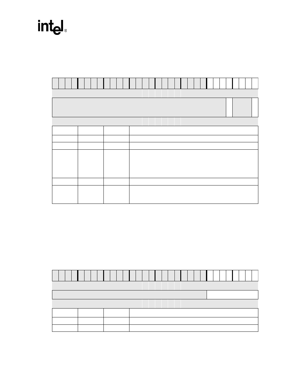
MSR Bit Definitions
Physical Address
0x4160_0018
Modem Status Reg. (MSR)
PXA26x Processor Family Hardware
UART
User
Settings
Bit
31 30 29 28 27 26 25 24 23 22 21 20 19 18 17 16 15 14 13 12 11 10 9
8
7
6
5
4
3
2
1
0
Reserved
CT
S
R
eser
ved
DC
T
S
Reset
?
?
?
?
?
?
?
?
?
?
?
?
?
?
?
?
?
?
?
?
?
?
?
?
?
?
?
1
?
?
?
0
Bits
Access
Name
Description
31:8
N/A
—
Reserved – Read as unknown and must be written as zero.
7:5
N/A
—
Reserved – Read as unknown and must be written as zero.
4
R
CTS
CLEAR TO SEND:
Complement of the Clear to Send (nCTS) input. Equivalent to MCR[RTS] if
MCR[LOOP] is set.
0 – nCTS pin is 1
1 – nCTS pin is 0
3:1
N/A
—
Reserved – Read as unknown and must be written as zero.
0
R
DCTS
DELTA CLEAR TO SEND:
0 – No change in nCTS pin since last read of MSR
1 – nCTS pin has changed state
Table 17-18.
SPR Bit Definitions
Physical Address
0x4160_001C
Scratchpad Reg. (SPR)
PXA26x Processor Family Hardware
UART
User
Settings
Bit
31 30 29 28 27 26 25 24 23 22 21 20 19 18 17 16 15 14 13 12 11 10 9
8
7
6
5
4
3
2
1
0
Reserved
Reset
?
?
?
?
?
?
?
?
?
?
?
?
?
?
?
?
?
?
?
?
?
?
?
?
0
0
0
0
0
0
0
0
Bits
Access
Name
Description
31:8
N/A
—
Reserved – Read as unknown and must be written as zero.
7:0
R
SPR[7:0]
No effect on UART function