Table 4-52. pwm_pervaln bit definitions, 3 pulse width modulator output wave example, Figure 4-4. basic pulse width waveform – Intel PXA26X User Manual
Page 155
Intel® PXA26x Processor Family Developer’s Manual
4-47
System Integration Unit
Note:
Due to internal timing requirements, all changes to any of the PWM registers must be complete a
minimum of 4 core clock cycles before the start of end of a PWM clock cycle in order to guarantee
that the following PWM cycle implements the new values.
shows the bitmap of the PWM Period Control registers.
4.5.3
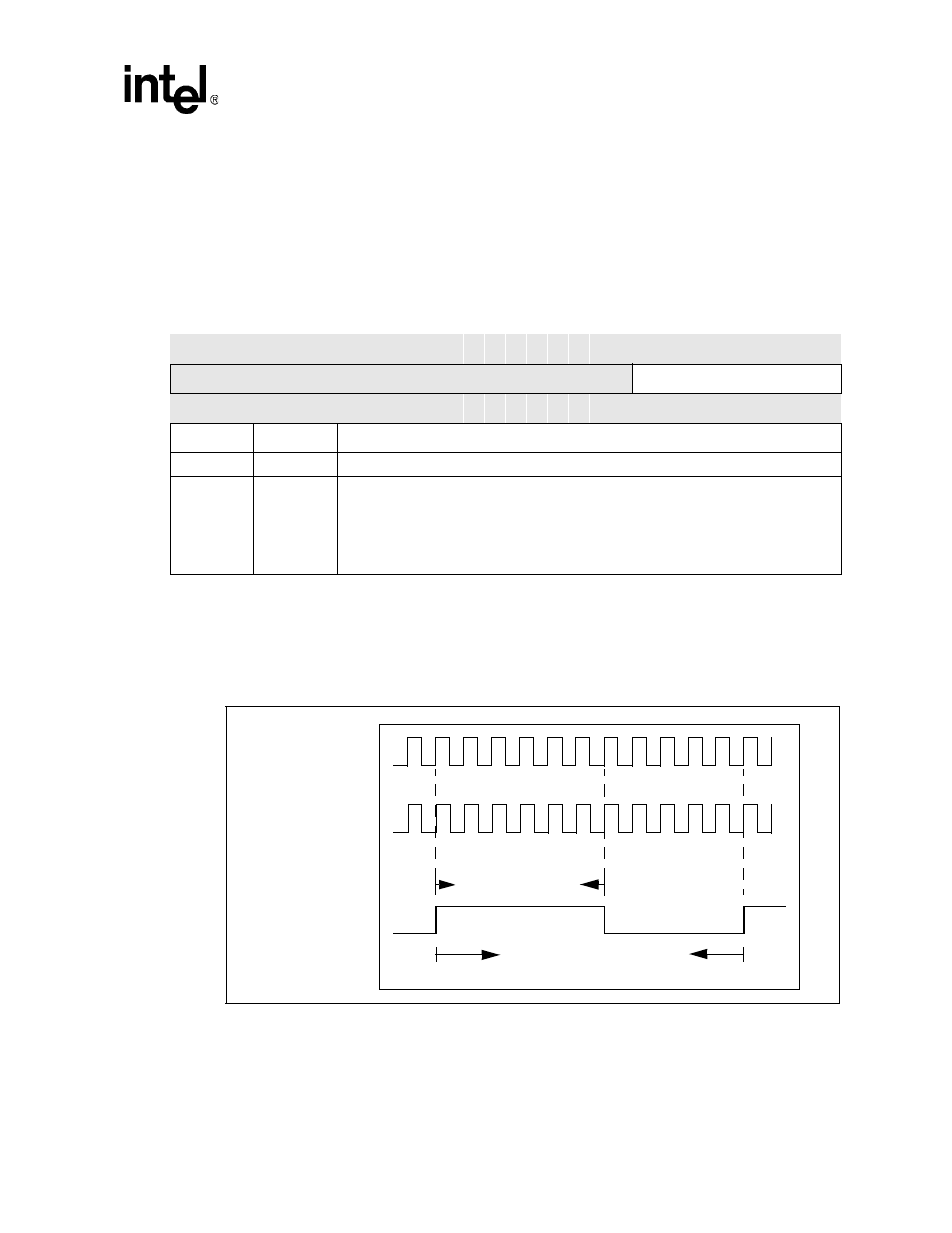
Pulse Width Modulator Output Wave Example
is an example of the output of a Pulse Width Modulator for reference.
PWM_PERVAL[PV] = 0xA
PWM_DUTY[FDCYCLE] = 0x0
PWM_DUTY[DCYCLE] = 0x6
PWM_CTRL[PRESCALE] = 0x0
Table 4-52. PWM_PERVALn Bit Definitions
Physical Address
0x40B0_0008
0x40C0_0008
PWM Period Control Registers
(PWM_PERVAL0, PWM_PERVAL1)
System Integration Unit
Bit
31 30 29 28 27 26 25 24 23 22 21 20 19 18 17 16 15 14 13 12 11 10 9
8
7
6
5
4
3
2
1
0
Reserved
PV
Reset
0
0
0
0
0
0
0
0
0
0
0
0
0
0
0
0
0
0
0
0
0
0
0
0
0
0
0
0
0
1
0
0
Bits
Name
Description
<31:10>
—
Reserved
<9:0>
PV
PWMn PERIOD CONTROL:
The number of PSCLK_PWMn cycles that comprise one PWM_OUTn cycle
NOTE: If PV = 0x0, the PWMn clock (PWM_OUTn) is set high and does not toggle unless
FDCYCLE = 0x0 and DCYCLE = 0x0. In this case PWM_OUTn is set low and
does not toggle regardless of the value in PV.
Figure 4-4. Basic Pulse Width Waveform
PWM_OUTn
PSCLK_PWMn
PWM_DUTYn = 6
PWM_PERVALn = 10 (+1)
3.6864 MHz