Intel PXA26X User Manual
Page 200
6-10
Intel® PXA26x Processor Family Developer’s Manual
Memory Controller
22:21
DRAC2[1:0]
SDRAM ROW ADDRESS BIT COUNT FOR PARTITION PAIR 2/3:
00 – 11 row address bits
01 – 12 row address bits
10 – 13 row address bits
11 – Reserved
20:19
DCAC2[1:0]
NUMBER OF COLUMN ADDRESS BITS FOR PARTITION PAIR 2/3:
00 – 8 column address bits
01 – 9 column address bits
10 – 10 column address bits
11 – 11 column address bits
18
DWID2
SDRAM DATA BUS WIDTH FOR PARTITION PAIR 2/3:
0 – 32 bits
1 – 16 bits
17
DE3
SDRAM ENABLE FOR PARTITION 3:
For each SDRAM partition, there is an enable bit. A single (non-burst) 32-bit (or 16-bit if
MDCNFG:DWID2=’1’) access (read or write) to a disabled SDRAM partition triggers a CBR
refresh cycle to all partitions. When all partitions are disabled, the refresh counter is
disabled.
0 – SDRAM partition disabled
1 – SDRAM partition enabled
16
DE2
SDRAM ENABLE FOR PARTITION 2:
For each SDRAM partition, there is an enable bit. A single (non-burst) 32-bit (or 16-bit if
MDCNFG:DWID2=’1’) access (read or write) to a disabled SDRAM partition triggers a CBR
refresh cycle to all partitions. When all partitions are disabled, the refresh counter is
disabled.
0 – SDRAM partition disabled
1 – SDRAM partition enabled
15:13
—
Reserved
12
DSA1111_0
USE SA-1111 ADDRESSING MUXING MODE FOR PAIR 0/1 – Setting this bit overrides
the addressing bit programmed in MDCNFG:DADDR0.
For an explanation on how the SA-1111 addressing works, see
11
DLATCH0
RETURN DATA FROM SDRAM LATCHING SCHEME FOR PAIR 0/1
0 – Reserved
1 – Latch return data with return clock
This bit must always be written with a ‘1’ to enable the return clock SDCLK for latching
data. For more detail on this return data latching.
10
DADDR0
Reserved
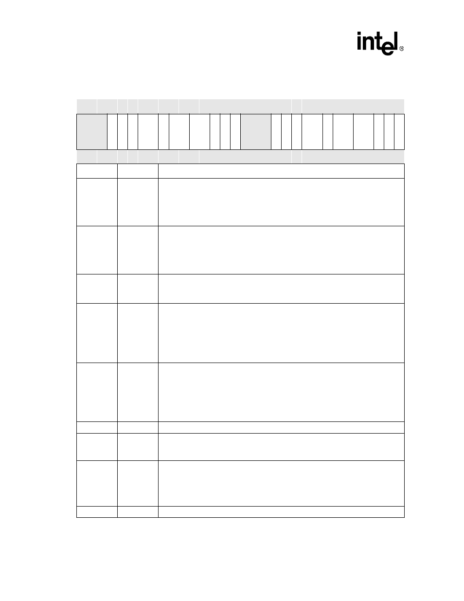
Table 6-3. MDCNFG Register Bitmap and Bit Definitions (Sheet 2 of 3)
0x4800 0000
MDCNFG
Bit
31 30 29 28 27 26 25 24 23 22 21 20 19 18 17 16 15 14 13 12 11 10 9
8
7
6
5
4
3
2
1
0
R
eser
ved
DS
A1
1
1
1
_
2
DL
A
T
CH
2
DA
DD
R2
DT
C
2
DN
B2
DR
AC
2
DC
AC
2
DW
ID
2
DE
3
DE
2
R
eser
ved
DS
A1
1
1
1
_
0
DL
A
T
CH
0
DA
DD
R0
DT
C
0
DN
B0
DR
AC
0
DC
AC
0
DW
ID
0
DE
1
DE
0
Reset
0
0
0
0
0
0
0
0
0
0
0
0
0
0
0
0
0
0
0
0
0
0
0
0
0
0
0
0
0
0
0
0
Bits
Name
Description