7 receive fifo occupancy register (for) – Intel PXA26X User Manual
Page 602
17-18
Intel® PXA26x Processor Family Developer’s Manual
Hardware UART
17.5.7
Receive FIFO Occupancy Register (FOR)
The Receive FIFO Occupancy Register shows the number of bytes currently remaining in the
receive FIFO. It can be used by the processor to determine the number of trailing bytes to remove.
The FOR is incremented once for each byte of data written to the receive FIFO and decremented
once for each byte read.
3
Write
TIL
TRANSMITTER INTERRUPT LEVEL:
Determines when interrupts or DMA requests are sent from the transmit
FIFO.
0 – Interrupt/DMA request when FIFO is half empty.
1 – Interrupt/DMA request when FIFO is empty
2
Write
RESETTF
RESET TRANSMITTER FIFO:
When RESETTF is set to 1, all the bytes in the transmitter FIFO are
cleared. The TDRQ bit in the LSR is set and the IIR shows a transmitter
requests data interrupt, if the TIE bit in the IER is set. The Transmitter Shift
Register is not cleared and it completes the current transmission.
0 – Writing 0 has no effect
1 – The transmitter FIFO is cleared
1
Write
RESETRF
RESET RECEIVER FIFO:
When RESETRF is set to 1, all the bytes in the receiver FIFO are cleared.
The DR bit in the LSR is reset to 0. All the error bits in the FIFO and the
FIFOE bit in the LSR are cleared. Any error bits, OE, PE, FE or BI, that had
been set in LSR are still set. The Receiver Shift Register is not cleared. If
the IIR had been set to received data available, it is cleared.
0 – Writing 0 has no effect
1 – The receiver FIFO is cleared
0
Write
TRFIFOE
TRANSMIT AND RECEIVE FIFO ENABLE:
TRFIFOE enables/disables the transmitter and receiver FIFOs. When
TRFIFOE = 1, both FIFOs are enabled (FIFO Mode). When TRFIFOE = 0,
the FIFOs are both disabled (non-FIFO Mode). Writing a 0 to this bit clears
all bytes in both FIFOs. When changing from FIFO mode to non-FIFO mode
and vice versa, data is automatically cleared from the FIFOs. This bit must
be 1 when other bits in this register are written or the other bits are not
programmed.
0 – FIFOs are disabled
1 – FIFOs are enabled
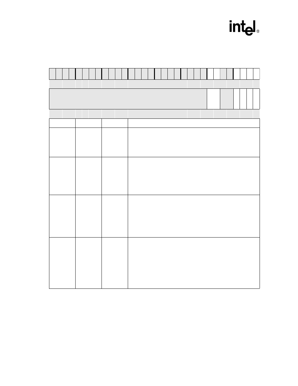
Table 17-10.
FCR Bit Definitions (Sheet 2 of 2)
Physical Address
0x4160_0008
FIFO Control Reg. (FCR)
PXA26x Processor Family Hardware
UART
User
Settings
Bit
31 30 29 28 27 26 25 24 23 22 21 20 19 18 17 16 15 14 13 12 11 10 9
8
7
6
5
4
3
2
1
0
Reserved
ITL
R
eser
ved
TIL
R
ESE
TTF
R
ESE
TRF
TR
FIF
O
E
Reset
?
?
?
?
?
?
?
?
?
?
?
?
?
?
?
?
?
?
?
?
?
?
?
?
0
0
?
?
0
0
0
0
Bits
Access
Name
Description