Intel PXA26X User Manual
Page 201
Intel® PXA26x Processor Family Developer’s Manual
6-11
Memory Controller
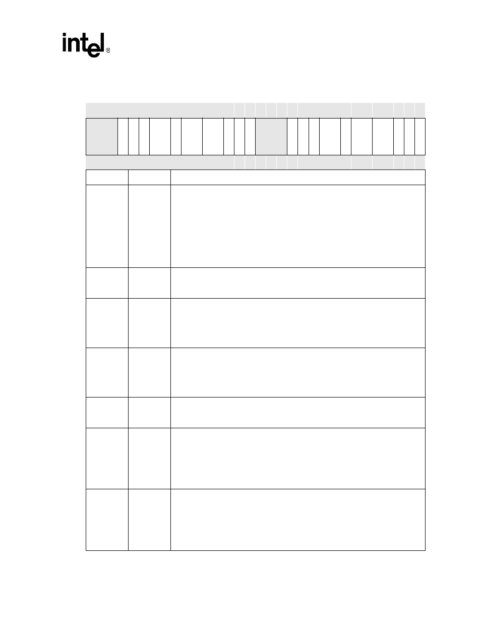
9:8
DTC0[1:0]
TIMING CATEGORY FOR SDRAM PAIR 0/1:
00 – tRP = 2 clks, CL = 2, tRCD = 1 clks, tRAS(min) = 3 clks, tRC = 4 clks
01 – tRP = 2 clks, CL = 2, tRCD = 2 clks, tRAS(min) = 5 clks, tRC = 8 clks
10 – tRP = 3 clks, CL = 3, tRCD = 3 clks, tRAS(min) =7 clks, tRC=10 clks
11 – tRP = 3 clks, CL = 3, tRCD = 3 clks, tRAS(min) = 7 clks, tRC = 11 clks
tWR (write recovery time) is fixed at 2 clocks.
Used to configure the SDRAM timings to the SDRAM manufacturer’s specifications. Clocks
referred to in the timings above are the number of SDCLKs. SDCLKs may not be
equivalent to memory clocks based on the MDREFRx[KxDB2].
7
DNB0
NUMBER OF BANKS IN LOWER PARTITION PAIR:
0 – 2 internal SDRAM banks
1 – 4 internal SDRAM banks
6:5
DRAC0[1:0]
SDRAM ROW ADDRESS BIT COUNT FOR PARTITION PAIR 0/1:
00 – 11 row address bits
01 – 12 row address bits
10 – 13 row address bits
11 – Reserved
4:3
DCAC0[1:0]
NUMBER OF COLUMN ADDRESS BITS FOR PARTITION PAIR 0/1:
00 – 8 column address bits
01 – 9 column address bits
10 – 10 column address bits
11 – 11 column address bits
2
DWID0
SDRAM DATA BUS WIDTH FOR PARTITION PAIR 0/1:
0 – 32 bits
1 – 16 bits
1
DE1
SDRAM ENABLE FOR PARTITION 1:
For each SDRAM partition, there is an enable bit. A single (non-burst) 32-bit (or 16-bit if
MDCNFG:DWID0=’1’) access (read or write) to a disabled SDRAM partition triggers a CBR
refresh cycle to all partitions. When all partitions are disabled, the refresh counter is
disabled.
0 – SDRAM partition disabled
1 – SDRAM partition enabled
0
DE0
SDRAM ENABLE FOR PARTITION 0:
For each SDRAM partition, there is an enable bit. A single (non-burst) 32-bit (or 16-bit if
MDCNFG:DWID0=’1’) access (read or write) to a disabled SDRAM partition triggers a CBR
refresh cycle to all partitions. When all partitions are disabled, the refresh counter is
disabled.
0 – SDRAM partition disabled
1 – SDRAM partition enabled
Table 6-3. MDCNFG Register Bitmap and Bit Definitions (Sheet 3 of 3)
0x4800 0000
MDCNFG
Bit
31 30 29 28 27 26 25 24 23 22 21 20 19 18 17 16 15 14 13 12 11 10 9
8
7
6
5
4
3
2
1
0
R
eser
ved
DS
A1
1
1
1
_
2
DL
A
T
CH
2
DA
DD
R2
DT
C
2
DN
B2
DR
AC
2
DC
AC
2
DW
ID
2
DE
3
DE
2
R
eser
ved
DS
A1
1
1
1
_
0
DL
A
T
CH
0
DA
DD
R0
DT
C
0
DN
B0
DR
AC
0
DC
AC
0
DW
ID
0
DE
1
DE
0
Reset
0
0
0
0
0
0
0
0
0
0
0
0
0
0
0
0
0
0
0
0
0
0
0
0
0
0
0
0
0
0
0
0
Bits
Name
Description