Table 4-9. gpsr0 bit definitions, Table 4-10. gpsr1 bit definitions – Intel PXA26X User Manual
Page 119
Intel® PXA26x Processor Family Developer’s Manual
4-11
System Integration Unit
4.1.3.3
GPIO Pin Output Set Registers (GPSR0, GPSR1, and GPSR2) and Pin
Output Clear Registers (GPCR0, GPCR1, GPCR2)
When a GPIO is configured as an output, you control the state of the pin by writing to either the
GPIO Pin Output Set registers (GPSR) or the GPIO Pin Output Clear registers (GPCR). An output
pin is set high by writing a one to its corresponding bit within the GPSR. To clear an output pin, a
one is written to the corresponding bit within the GPCR. GPSR and GPCR are write-only registers.
Reads return unpredictable values.
Writing a zero to any of the GPSR or GPCR bits has no effect on the state of the pin. Writing a one
to a GPSR or GPCR bit corresponding to a pin that is configured as an input is effective only after
the pin is configured as an output. Reserved bits (GPSR2[31:26] and GPCR2[31:26]), must be
written with zeros and reads must be ignored.
, and
show the bitmaps of GPSR0, GPSR1, and GPSR2.
, and
show the bitmaps of GPCR0, GPCR1, and GPCR2.
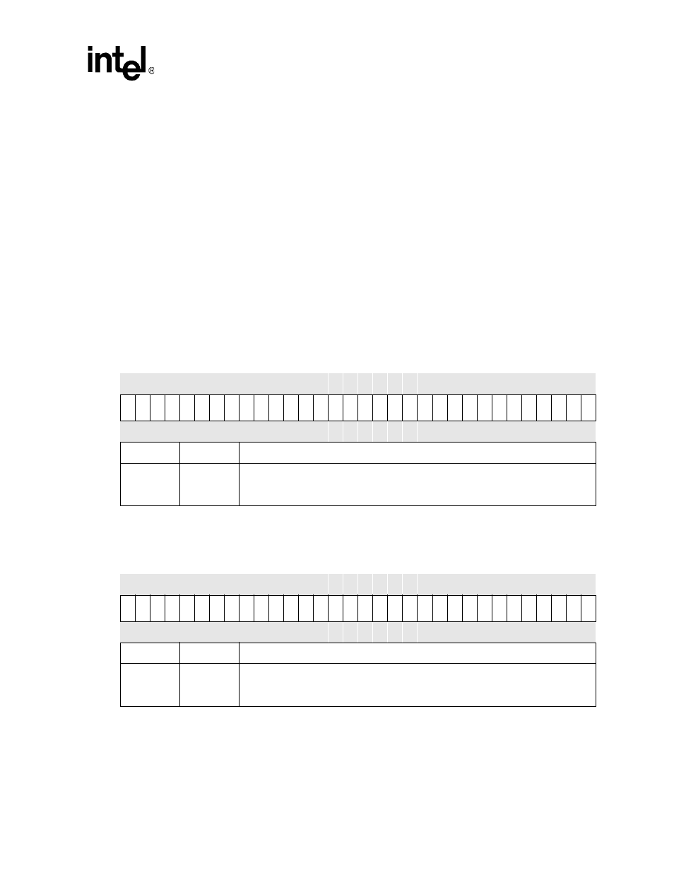
Table 4-9. GPSR0 Bit Definitions
Physical Address
0x40E0_0018
GPSR0
System Integration Unit
Bit
31 30 29 28 27 26 25 24 23 22 21 20 19 18 17 16 15 14 13 12 11 10 9
8
7
6
5
4
3
2
1
0
PS
3
1
PS
3
0
PS
2
9
PS
2
8
PS
2
7
PS
2
6
PS
2
5
PS
2
4
PS
2
3
PS
2
2
PS
2
1
PS
2
0
PS
1
9
PS
1
8
PS
1
7
PS
1
6
PS
1
5
PS
1
4
PS
1
3
PS
1
2
PS1
1
PS
1
0
PS
9
PS
8
PS
7
PS
6
PS
5
PS
4
PS
3
PS
2
PS
1
PS
0
Reset
0
0
0
0
0
0
0
0
0
0
0
0
0
0
0
0
0
0
0
0
0
0
0
0
0
0
0
0
0
0
0
0
Bits
Name
Description
<31:0>
PS[x]
GPIO Pin ‘x’ Output Pin Set (where x = 0 through 31).
0 – Pin level unaffected.
1 – If pin configured as an output, set pin level high (one).
Table 4-10. GPSR1 Bit Definitions
Physical Address
0x40E0_001C
GPSR1
System Integration Unit
Bit
31 30 29 28 27 26 25 24 23 22 21 20 19 18 17 16 15 14 13 12 11 10 9
8
7
6
5
4
3
2
1
0
PS
6
3
PS
6
2
PS
6
1
PS
6
0
PS
5
9
PS
5
8
PS
5
7
PS
5
6
PS
5
5
PS
5
4
PS
5
3
PS
5
2
PS
5
1
PS
5
0
PS
4
9
PS
4
8
PS
4
7
PS
4
6
PS
4
5
PS
4
4
PS
4
3
PS
4
2
PS
4
1
PS
4
0
PS
3
9
PS
3
8
PS
3
7
PS
3
6
PS
3
5
PS
3
4
PS
3
3
PS
3
2
Reset
0
0
0
0
0
0
0
0
0
0
0
0
0
0
0
0
0
0
0
0
0
0
0
0
0
0
0
0
0
0
0
0
Bits
Name
Description
<31:0>
PS[x]
GPIO Pin ‘x’ Output Pin Set (where x = 32 through 63).
0 – Pin level unaffected.
1 – If pin configured as an output, set pin level high (one).