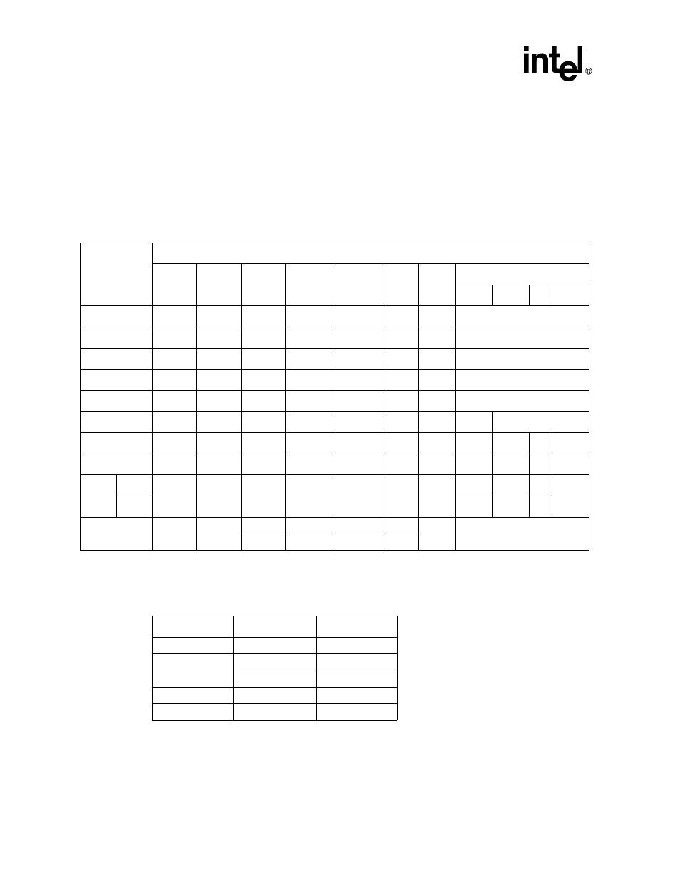
Table 6-12. sdram command encoding, Table 6-13. sdram mode register opcode table – Intel PXA26X User Manual
Page 216

6-26
Intel® PXA26x Processor Family Developer’s Manual
Memory Controller
•
Power-Down (PWRDN)
•
Enter Self-Refresh (SLFRSH)
•
Exit Power-Down (PWRDNX)
•
No Operation (NOP)
shows the SDRAM interface commands. The table assumes the bank bits for the
SDRAM are sent out on external address lines MA<24:23>.
The programmable opcode for address bits MA<24:17> used during the mode-register set
command (MRS) is exactly what is programmed in the MDMRS register.
Table 6-12. SDRAM Command Encoding
Command
Pins
SDCKE
(at clk
n-1)
SDCKE
(at clk
n)
nSDCS
3:0
nSDRAS
nSDCAS
nWE
DQM
3:0
MA <24:10>
24:23
22:21
20
19:10
PWRDN
1
0
1
1
1
1
1
x
PWRDNX
0
1
1
1
1
1
1
x
SLFRSH
1
0
0
0
0
1
0
x
CBR
1
1
0
0
0
1
x
x
MRS
1
x
0
0
0
0
0
OP code
ACT
1
x
0
0
1
1
x
bank
row
READ
1
x
0
1
0
1
0
bank
col
0
col
WRITE
1
x
0
1
0
0
mask
bank
col
0
col
PALL
PRE
All
1
x
0
0
1
0
x
x
x
1
x
Bank
bank
0
NOP
1
x
1
x
x
x
x
x
0
1
1
1
Table 6-13. SDRAM Mode Register Opcode Table
Address Bits
Option
Value
MA<24:17>
Reserved
MDMRSx
MA[16:14]
CAS Latency = 2
010
CAS Latency = 3
011
MA[13]
Sequential Burst
0
MA[12:10]
Burst Length = 4
010
