Intel PXA26X User Manual
Page 236
6-46
Intel® PXA26x Processor Family Developer’s Manual
Memory Controller
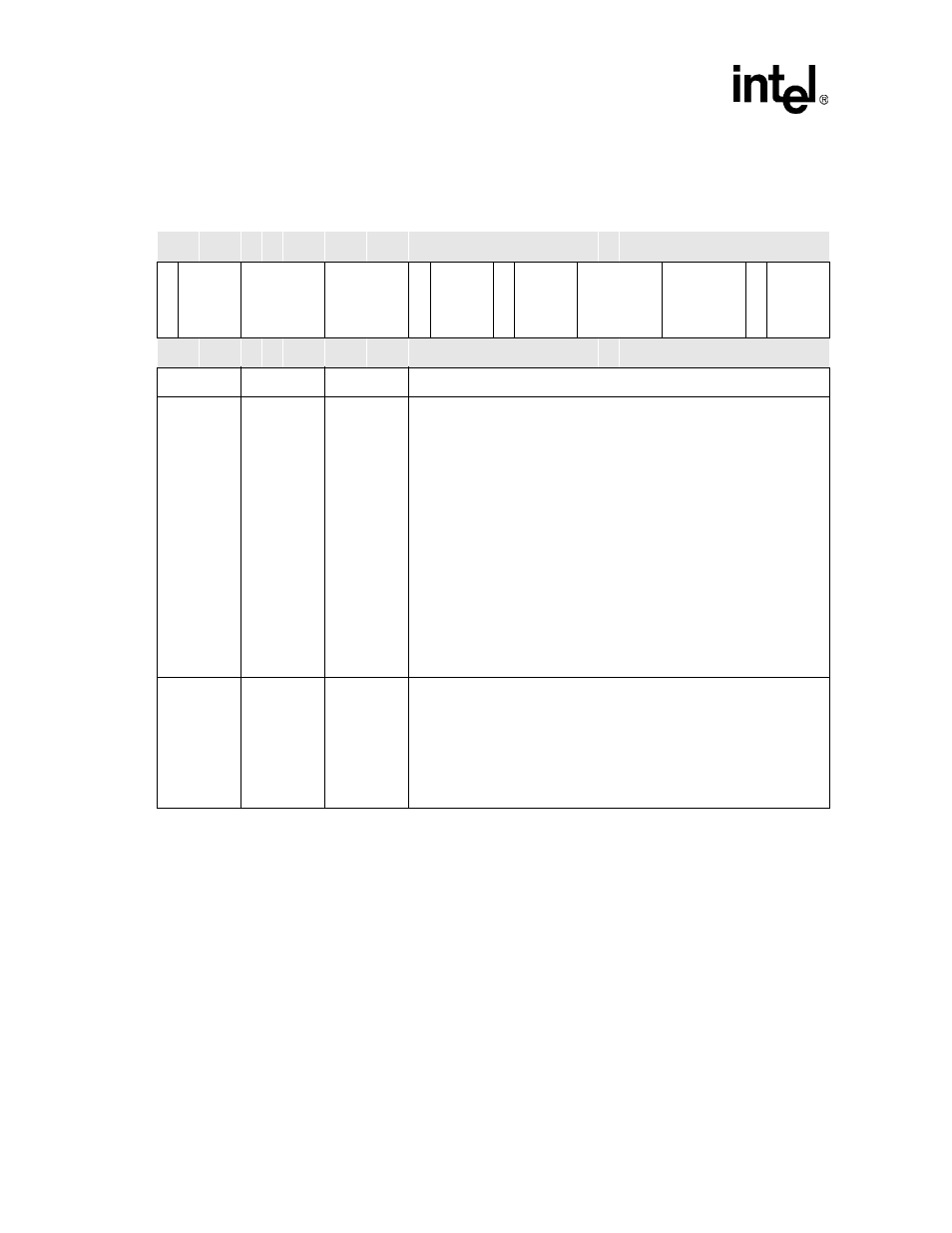
7:4
Read/Write
RDFx<3:0>
ROM DELAY FIRST ACCESS:
RDF programmed RDF value interpreted
0 – 11
0 – 11
12
13
13
15
14
18
15
23
Address to data valid for the first read access from all devices except VLIO
is equal to (RDFx + 2) memclks.
Address to data valid for subsequent read accesses to non-burst devices is
equal to (RDFx + 1) memclks.
nWE assertion for write accesses (which are non-burst) to all flash is equal
to (RDFx + 1) memclks.
nOE (nPWE) assert time for each beat of read (write) is equal to (RDFx + 1)
memclks for Variable Latency I/O (nCS[5:0]). For variable latency I/O, RDFx
must be greater than or equal to 3.
3
Read/Write
RBWx
ROM BUS WIDTH:
0 – 32 bits
1 – 16 bits
For reset value for RBW0, see
This value must be programmed with all memory types including
Synchronous Static Memory.
This value must not change during normal operation.
Table 6-25. MSC0/1/2 Register Bit Definitions (Sheet 2 of 3)
0X4800 0008/
0x4800 000C/
0x4800 0010
MSC0/
MSC1/
MSC2
processor
Bit
31 30 29 28 27 26 25 24 23 22 21 20 19 18 17 16 15 14 13 12 11 10 9
8
7
6
5
4
3
2
1
0
R
B
U
FF1/3/5
RR
R1
/3
/5
RD
N1
/3
/5
RD
F
1
/3
/5
R
B
W1/3/5
R
T
1/3/5
R
B
U
FF0/2/4
RR
R0
/2
/4
RD
N0
/2
/4
RD
F
0
/2
/4
R
B
W0/2/4
R
T
0/2/4
Reset
0
1
1
1
1
1
1
1
1
1
1
1
0
0
0
0
0
1
1
1
1
1
1
1
1
1
1
1
*
0
0
0
Bits
Access
Name
Description