Table 2-3. pxa26x processor family id values, 5 coprocessor 15 register 1 - p-bit, 4 input/output ordering – Intel PXA26X User Manual
Page 35: 5 coprocessor 15 register 1 – p-bit
Intel® PXA26x Processor Family Developer’s Manual
2-5
System Architecture
2.3.5
Coprocessor 15 Register 1 – P-Bit
Bit 1 of this register is defined as the Page Table Memory Attribute bit or P-bit. It is not
implemented in the processor and must be written as zero. Similarly, the P-bit in the page table
descriptor in the Memory Management Unit (MMU) is not implemented and must be written to
zero.
2.4
Input/Output Ordering
The processor uses queues that accept memory requests from the three internal masters: core,
DMA controller, and LCD controller. Operations issued by a master are completed in the order
they were received. Operations from one master may be interrupted by operations from another
master. The processor does not provide a method to regulate the order of operations from different
masters.
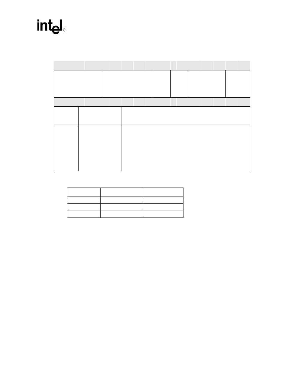
[9:4]
Product Number
This field is specific to each ASSP.
Product Number
0b010000 = PXA26x processor family
[3:0]
Product Revision
This field tracks the different steppings for each ASSP.
Product Revision
0b0000 – Reserved
0b0001 – Reserved
0b0010 – Reserved
0b0011 – A0 Stepping
0b0101 – B0 Stepping
0b0110 – B1 Stepping
Table 2-3. PXA26x processor family ID Values
Stepping
ARM* ID
JTAG ID
A0
0x69052903
0x39264013
B0
0x69052D05
0x59264013
B1
0x69052D06
0x69264013
Table 2-2. ID Register Bitmap and Bit Definitions (Read-only) (Sheet 2 of 2)
CP15 Register 0
ID
CP15
Bit
31 30 29 28 27 26 25 24 23 22 21 20 19 18 17 16 15 14 13 12 11 10 9
8
7
6
5
4
3
2
1
0
Im
plem
e
n
tation
T
radem
ar
k
Arc
h
it
e
c
tu
re
Ve
rs
io
n
Co
re
gener
ati
o
n
Co
re
R
e
vi
sion
P
ro
duct
N
u
m
ber
P
ro
duct
R
e
vi
sion
Reset
0
1
1
0
1
0
0
1
0
0
0
0
0
1
0
1
0
0
1
0
1
1
0
1
0
0
0
0
0
1
0
1