Table 4-4. gplr1 bit definitions, Table 4-5. gplr2 register bitmap, Table 4-4 – Intel PXA26X User Manual
Page 117: Table 4-5
Intel® PXA26x Processor Family Developer’s Manual
4-9
System Integration Unit
This is read/write register. Ignore reads from reserved bits. Write zeros to reserved bits.
4.1.3.2
GPIO Pin Direction Registers (GPDR0, GPDR1, GPDR2)
Whether a pin is an input or an output is controlled by programming the GPIO Pin Direction
registers (GPDR0, GPDR1, GPDR2). The GPDR registers contain one direction control bit for
each of the 90 GPIO pins. For GPIO[85:0], if a direction bit is programmed to a one, the GPIO is
an output. If it is programmed to a zero, it is an input. For GPIO[89:86], if a direction bit is
programmed to a one, the GPIO is an input. If it is programmed to a zero, it is an output. Reserved
bits (GPDR2[31:26]), must be written to zeros and reads to the reserved bits must be ignored.
Note:
A reset clears all bits in the GPDR0-2 registers and configures GPIO[85:0] as inputs and
GPIO[89:86] as outputs.
, and
show the bitmaps of the GPIO Pin Direction registers.
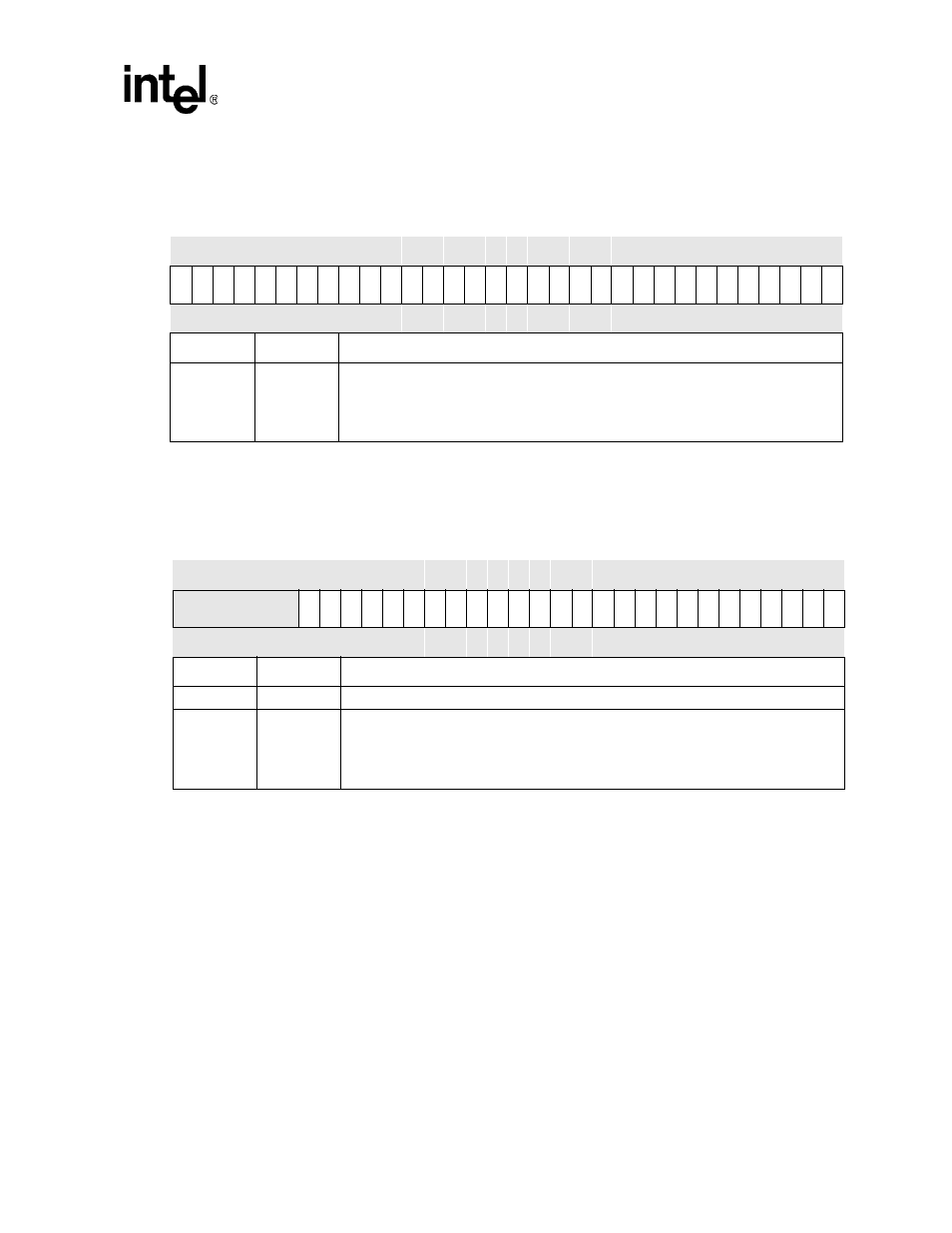
Table 4-4. GPLR1 Bit Definitions
Physical Address
0x40E0_0004
GPLR1
System Integration Unit
Bit
31 30 29 28 27 26 25 24 23 22 21 20 19 18 17 16 15 14 13 12 11 10 9
8
7
6
5
4
3
2
1
0
PL6
3
PL6
2
PL6
1
PL6
0
PL5
9
PL5
8
PL5
7
PL5
6
PL5
5
PL5
4
PL5
3
PL5
2
PL5
1
PL5
0
PL4
9
PL4
8
PL4
7
PL4
6
PL4
5
PL4
4
PL4
3
PL4
2
PL4
1
PL4
0
PL3
9
PL3
8
PL3
7
PL3
6
PL3
5
PL3
4
PL3
3
PL3
2
Reset
0
0
0
0
0
0
0
0
0
0
0
0
0
0
0
0
0
0
0
0
0
0
0
0
0
0
0
0
0
0
0
0
Bits
Name
Description
<31:0>
PL[x]
GPIO Pin Level ‘x’ (where x = 32 to 63).
This read-only field indicates the current value of each GPIO.
0 – Pin state is low
1 – Pin state is high
Table 4-5. GPLR2 Register Bitmap
Physical Address
0x40E0_0008
GPIO Pin Level Register2 (GPLR2)
System Integration Unit
Bit
31 30 29 28 27 26 25 24 23 22 21 20 19 18 17 16 15 14 13 12 11 10 9
8
7
6
5
4
3
2
1
0
Reserved
PL8
9
PL8
8
PL8
7
PL8
6
PL8
5
PL8
4
PL8
3
PL8
2
PL8
1
PL8
0
PL7
9
PL7
8
PL7
7
PL7
6
PL7
5
PL7
4
PL7
3
PL7
2
PL7
1
PL7
0
PL6
9
PL6
8
PL6
7
PL6
6
PL6
5
PL6
4
Reset
0
0
0
0
0
0
0
0
0
0
0
0
0
0
0
0
0
0
0
0
0
0
0
0
0
0
0
0
0
0
0
0
Bits
Name
Description
<31:26>
—
Reserved
<25:0>
PL[x]
GPIO Pin Level ‘x’ (where x = 64 to 89).
This read-only field indicates the current value of each GPIO.
0 – Pin state is low
1 – Pin state is high