6 synchronous dram memory interface, 1 sdram mdcnfg register – Intel PXA26X User Manual
Page 199
Intel® PXA26x Processor Family Developer’s Manual
6-9
Memory Controller
6.6
Synchronous DRAM Memory Interface
Each possible SDRAM portion of the Memory Map is referred to as a partition, to distinguish them
from banks internal to SDRAM devices.
The signals used to control the SDRAM memory are listed in
Section 6.2.1, “SDRAM Interface
6.6.1
SDRAM MDCNFG Register
MDCNFG is a read/write register and contains control bits for configuring the SDRAM. Both
SDRAM partitions in a pair (0/1 or 2/3) must be implemented with the same type of SDRAM
devices, but the two partition pairs may differ. Refer to
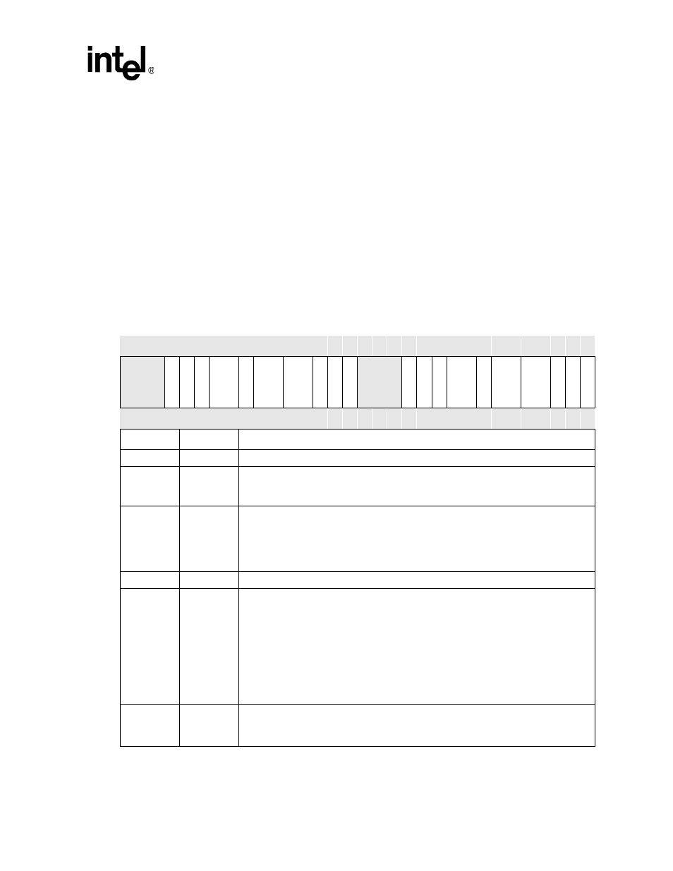
Table 6-3. MDCNFG Register Bitmap and Bit Definitions (Sheet 1 of 3)
0x4800 0000
MDCNFG
Bit
31 30 29 28 27 26 25 24 23 22 21 20 19 18 17 16 15 14 13 12 11 10 9
8
7
6
5
4
3
2
1
0
R
eser
ved
D
S
A
1
1
1
1_2
DL
A
T
CH
2
DAD
DR
2
DT
C
2
DN
B2
DR
AC
2
DC
AC
2
DW
ID
2
DE
3
DE
2
R
eser
ved
D
S
A
1
1
1
1_0
DL
A
T
CH
0
DAD
DR
0
DT
C
0
DN
B0
DR
AC
0
DC
AC
0
DW
ID
0
DE
1
DE
0
Reset
0
0
0
0
0
0
0
0
0
0
0
0
0
0
0
0
0
0
0
0
0
0
0
0
0
0
0
0
0
0
0
0
Bits
Name
Description
31:29
—
Reserved
28
DSA1111_2
SA-1111 ADDRESSING MUXING MODE FOR PAIR 2/3 – Setting this bit overrides the
addressing bit programmed in MDCNFG:DADDR2.
For an explanation on how the SA-1111 addressing works, see
.
27
DLATCH2
RETURN DATA FROM SDRAM LATCHING SCHEME FOR PAIR 2/3:
0 – Reserved
1 – Latch return data with return clock
This bit must always be written with a ‘1’ to enable using the return clock SDCLK for
latching data. For more detail on this return data latching.
26
DADDR2
Reserved
25:24
DTC2[1:0]
TIMING CATEGORY FOR SDRAM PAIR 2/3:
00 – tRP = 2 clks, CL = 2, tRCD = 1 clks, tRAS(min) = 3 clks, tRC = 4 clks
01 – tRP = 2 clks, CL = 2, tRCD = 2 clks, tRAS(min) = 5 clks, tRC = 8 clks
10 – tRP = 3 clks, CL = 3, tRCD = 3 clks, tRAS(min) =7 clks, tRC=10 clks
11 – tRP = 3 clks, CL = 3, tRCD = 3 clks, tRAS(min) = 7 clks, tRC = 11 clks
tWR (write recovery time) is fixed at 2 clocks.
These bits are used to configure the SDRAM timings per the SDRAM manufacturer’s
specifications. Clocks referred to in the timings above are the number of SDCLKs. SDCLKs
may not be equivalent to memory clocks based on the MDREFRx[KxDB2].
23
DNB2
NUMBER OF BANKS IN UPPER PARTITION PAIR:
0 – 2 internal SDRAM banks
1 – 4 internal SDRAM banks