Intel PXA26X User Manual
Page 46
2-16
Intel® PXA26x Processor Family Developer’s Manual
System Architecture
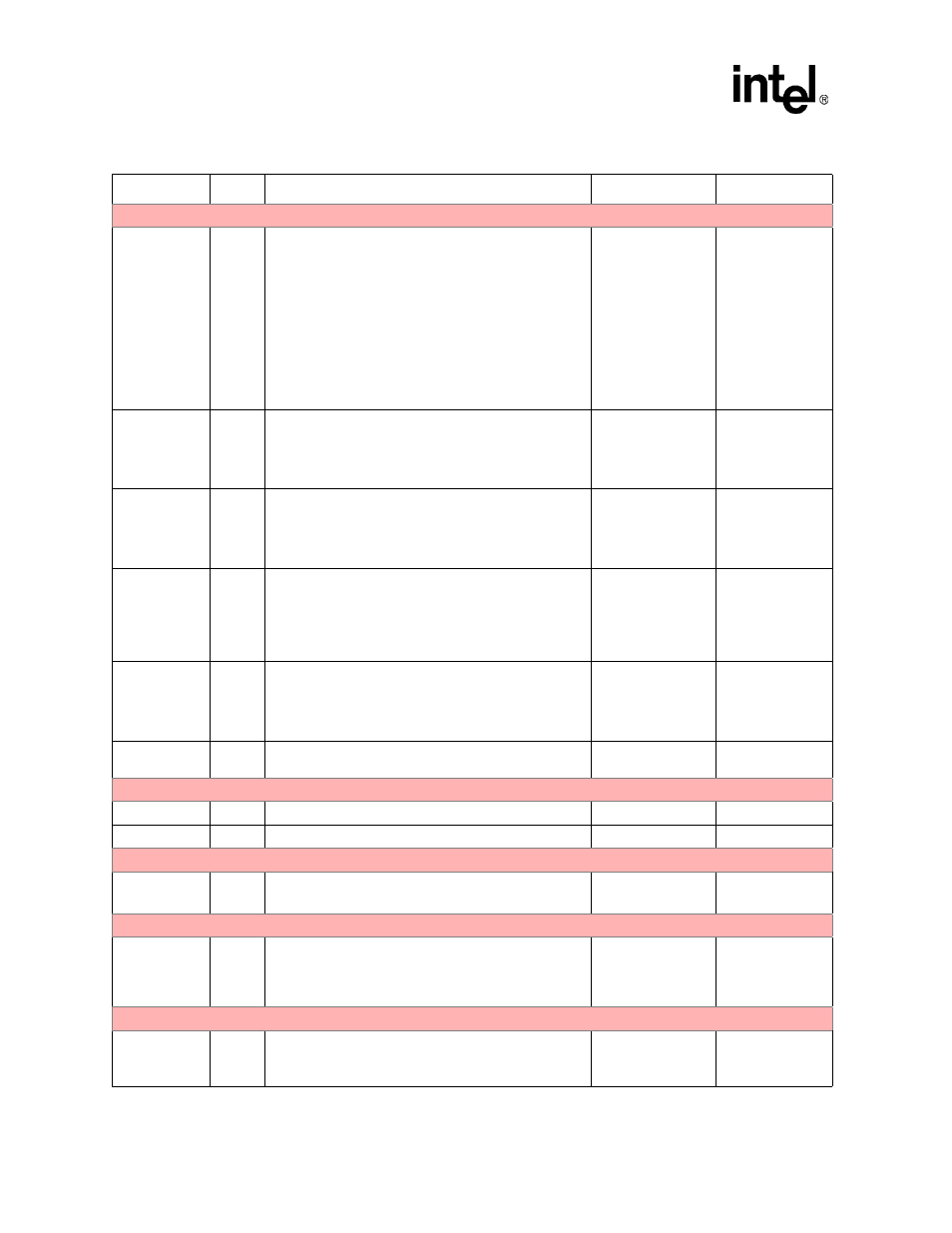
AC97 Controller and I2S Controller Pins
BITCLK/
GPIO[28]
ICOCZ
AC97 AUDIO PORT BIT CLOCK (input):
AC97 clock is generated by Codec 0 and fed into the
PXA26x processor family and Codec 1.
AC97 AUDIO PORT BIT CLOCK (output):
AC97 clock is generated by the PXA26x processor family.
I2S BIT CLOCK (input):
I2S clock is generated externally and fed into PXA26x
processor family.
I2S BIT CLOCK (output):
I2S clock is generated by the PXA26x processor family.
Pulled High
Note [1]
Note [3]
SDATA_IN0/
GPIO[29]
ICOCZ
AC97 AUDIO PORT DATA IN (input):
Input line for Codec 0.
I2S DATA IN (input):
Input line for the I2S Controller.
Pulled High
Note [1]
Note [3]
SDATA_IN1/
GPIO[32]
ICOCZ
AC97 AUDIO PORT DATA IN (input):
Input line for Codec 1.
I2S SYSTEM CLOCK (output):
System clock from I2S Controller.
Pulled High
Note [1]
Note [3]
SDATA_OUT/
GPIO[30]
ICOCZ
AC97 AUDIO PORT DATA OUT (output):
Output from the PXA26x processor family to Codecs 0 and
1.
I2S DATA OUT (output):
Output line for the I2S Controller.
Pulled High
Note [1]
Note [3]
SYNC/
GPIO[31]
ICOCZ
AC97 AUDIO PORT SYNC SIGNAL (output):
Frame sync signal for the AC97 Controller.
I2S SYNC (output):
Frame sync signal for the I2S Controller.
Pulled High
Note [1]
Note [3]
nACRESET/
GPIO[89]
ICOC
AC97 AUDIO PORT RESET SIGNAL (output)
Driven Low
(but see Note[8])
Driven Low (but see
Note[8])
I2C Controller Pins
SCL
ICOCZ
I2C CLOCK (bidirectional)
Hi-Z
Hi-Z
SDA
ICOCZ
I2C DATA (bidirectional).
Hi-Z
Hi-Z
PWM Pins
PWM[1:0]/
GPIO[17:16]
ICOCZ
PULSE WIDTH MODULATION CHANNELS 0 AND 1
(outputs)
Pulled High
Note [1]
Note [3]
DMA Pins
DREQ[1:0]/
GPIO[19:20]
ICOCZ
DMA REQUEST (input):
Notifies the DMA Controller that an external device
requires a DMA transaction. DREQ[1] is GPIO[19].
DREQ[0] is GPIO[20].
Pulled High
Note [1]
Note [3]
GPIO Pins
GPIO[1:0]
ICOCZ
GENERAL PURPOSE I/O:
Walk-up sources on both rising and falling edges on
nRESET.
Pulled High
Note [1]
Note [3]
Table 2-6. Pin & Signal Descriptions for the PXA26x Processor Family (Sheet 8 of 12)
Pin Name
Type
Signal Descriptions
Reset State
Sleep State